Download
1 / 39
420 likes | 556 Vues
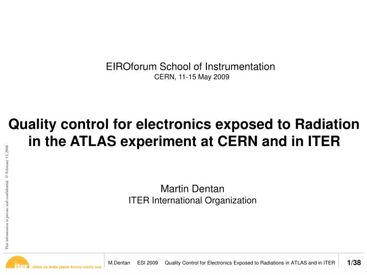
EIROforum School of Instrumentation CERN, 11-15 May 2009. Quality control for electronics exposed to Radiation in the ATLAS experiment at CERN and in ITER. Martin Dentan ITER International Organization. Outline. Radiation issues The ATLAS approach ATLAS experiment

E N D
EIROforum School of Instrumentation CERN, 11-15 May 2009 Quality control for electronics exposed to Radiation in the ATLAS experiment at CERN and in ITER Martin Dentan ITER International Organization
Outline • Radiation issues • The ATLAS approach • ATLAS experiment • Radiation hardness assurance • Examples of radiation test results • Summary • The ITER approach • ITER Project • Radiation hardness assurance
Radiation issues • 2 families: cumulated effects, and instantaneous (single event effects) • Cumulated effects • Total Ionizing Dose (TID) • Energy deposited in the electronics by radiation in the form of ionisation. • Unit: Gray (Gy), 1 Gy = 100 rad = 1 joule / kg. • Affects all electronics devices • Non-Ionizing Energy Loss (NIEL) • Displacement damage, mainly due to hadrons (n, p, p, …) • Unit : particles / cm2 • Energy dependent → normalized to 1 MeV neutrons equivalent / cm2. • Bipolar JT, LEDs, lasers, CCDs, optocouplers, photo-BJTs,… are affected • CMOS are not affected (majority carriers)
Radiation issues (2) • Single Event Effects (SEE) • Destructive effects: • SEL (Single Event Latch-up) • SEB (Single Event Burnout • SEGR (Single Event Gate Rupture • … • Transient effects: upsets • SEU : Single Event Upset (logic) • SET : Single Event Transient (linear) • SEEs are instantaneous effect • May occur just after the beam is switched on
Radiation issues : TID (total ionizing dose) • Mechanism : charge trapping in oxides and interfaces • => threshold voltage (Vt) shift, leakage current, noise, … • Example: leakage current and Vt shift induced in NMOS by total dose
Radiation issues : NIEL (Non-Ionizing Energy Loss) • Mechanism : bulk defects in semiconductors • => decrease of BJT gain b, noise, … • Cumulated damage => delayed effect • Example: dependance of BJT gain decrease on base thickness (lateral, power, phototransistors)
b e o e e Radiation issues : SEE (Single Event Effects) Example : Single Event Burnout
L’anneau LHC et les 4 expériences LHC experiments ATLAS 80 m under ground level LHC beams 2 proton beams in opposite direction Energy: 7 TeV – 7 TeV Luminosity: 1034 p.cm-2.s-1 Repetition rate: 40 MHz The LHC ring and the 4 experiments
LHC experiment: ATLAS • International collaboration, about 1900 people from ~150 institutions from 34 partner countries (incl. EU, US, Japan, Russia, Israel, Brazil, …) • 300 millions Euros among which 75 millions Euros for electronics • One of the two largest detector of the LHC experiments • 15 main systems, each of them containing electronics muon chambers Inner detectors (TRT, silicon trackers, silicon pixels) 24 m Proton beam Proton beam Electromagnetic LAr calorimeter Toroid magnets Hadronic calorimeter shielding 48 m
TID 1 MGy (Pixels) 2 Gy (Cavern) NIEL 4.1014 n.cm-2 (Pixels) 5.1010 n.cm-2 (Cavern) SEE 4.1014 h.cm-2 (Pixels) 1.1010 h.cm-2 (Cavern) hadrons > 20 MeV Radiation constraints (10 years) Simulations tools : FLUKA and G3-CALOR Front-end electronics (readout and pre-treatment) and some of the power supplies cannot be installed remotly (away from radiation), and cannot be shielded (it must be as transparent as possible to avoid shadows or parasitic images on particle detectors)
ATLAS systems Toroidal magnets (supra) shielding man muon detectors
ATLAS systems muon detectors Toroidal magnets (supra)
ATLAS systems hadroniccalorimeter shielding muon detectors
ATLAS systems Man hadronic calorimeter Man Muon detectors Toroidal Magnets (supra)
ATLAS policy on radiation tolerant electronics • Goal: reliability of the experiment with respect to radiation • Estimated lifetime of components must cover foreseen lifetime of LHC experiments, or at least a large fraction of it. • Rates of transient or destructive SEE must be acceptable. • Safety systems must remain always functionnal. • Mandatory for each sub-system of the experiment • Particular attention was paid to the identification of critical elements and to their possible failure modes. • Coherent approach • Same rules for every system • Based on recognized test methods • E.g. US-DOD MIL-STD-883E ; ESA SCC basic spec. No 22900 and 25100 • Simple, efficient and cost-effective
Main procedure Content: • Strategy for electronics procurement (ASICs, COTS) • Radiation Tolerance Criteria • Radiation Test Methods • Lists of radiation facilities • Standard test report form • (…)
Formal review for each component / system, based on acceptance criteria from APRTE • ATLAS Rad. Task Force • Simulate radiation levels • ATLAS tech. coordination / electronics / rad.hard.assurance • Tutorial course • Develop APRTE • Coordinate APRTE execution • Revues of rad test results • Technical support to partner labs • - Advices for component pre-selection • - Organisation of rad-test campaigns • - Analyse of results of tests, … • Rad. Working Group • develop & launch APRTE • ATLAS • Executive Board • Approve APRTE* • Collab. S2 • (…) • Collaboration S1 • Develop system S1 • coordinate fabrication of S1 • coordinate assembly of S1 Etc. • Lab. in charge of sub-system S1.1 • Develop S1.1 • Manufacture & test S1.1 • Radiation tests on S1.1 Etc. • Lab. S1.2 • (…) ATLAS PARTNER LABORATORIES * APRTE = ATLAS Policy on Radiation Tolerant Electronics Organisation ATLAS MANAGEMENT
Tutorial course • To establish a basic knowledge on radiation effects on electronics • - Part 1 : Radiation effects on electronic components • Radiation effects on materials (semiconductors, insulators, etc.) • Radiation units • Radiation effects on electronic devices • Part 2 : Radiation effects on electronic circuits • Cumulated radiation effects on digital and analog circuits • Single event effects on digital and analogue circuits • Examples of mitigation technics • Course given in 2000 to the LHC partners at CERN • and to several ATLAS Partner Institutes • Updated version given in 2006 at JET to EFDA Associations : • http://www.jet.efda.org/seminars/2006/060323dentan.pdf (part 1) • http://www.jet.efda.org/seminars/2006/060720dentan.pdf (part 2)
Radiation levels map Example: Total Ionizing Dose Muon chambers Hadronic calorimeter Electromagnetic Calorimeter Inner detectors
Radiation Tolerance Criteria Table of safety factors Table of raw simulated radiation levels • Safety factors representing: • Simulation inaccuracy; • Low dose rate effects • batch-to-batch variations • Simulated radiation levels: • For each location; • For each type of radiation • (TID, NIEL, SEE) Radiation Tolerance Criteria to be used for radiation tests
ATLAS electronics * ASIC = Application Specific Integrated Circuit
Technologies used for rad-hard ASICs • DMILL CMOS-NPN-PJFET SOI technology (radiation-hard) • Developed by CEA and produced by ATMEL for LHC and other applications • > 10 Mrads and > 3.1014 n/cm2 ; reduced SEE sensitivity • 0.25 mm CMOS bulk technology (standard) • Thin gate oxide => almost no Vt shift • Radiation tolerant layout • (closed gate structure, etc.) => no leakage current • > several 10 Mrads and > several 1014 n/cm2 • with radiation tolerant layout active silicon insulator substrate S G D Principle of closed gate structure
Procurement strategy • Whenever possible: • - Remove electronics from radiation and purchase standard electronics. • - Otherwise, apply following strategy: • Radiation tolerant COTS: • 1. Determine radiation level in the application (tables of simulated radiation levels) • Calculate the Radiation Tolerance Criteria (using ATLAS safety factors) • Pre-select generic components (radiation tests) • Purchase batches of pre-selected generic components • Qualify batches of components (radiation tests) • - Radiation tests can be made on individual components or on boards • - Special agreements with vendors may allow purchasing qualified batches only • Radiation-hard ASICs: • 1. Determine the radiation level in the application • Calculate the Radiation Tolerance Criteria • Select a radiation hard technology (DMILL or CMOS 0.25 mm + rad-tol layout) • Develop prototype ASIC and qualify the design (radiation test) • Qualifybatches of components(radiation tests) • Purchase qualified batches
ATLAS standard radiation test methods TID test method for qualification of batches of CMOS components Radiation tests must be normalized: • to be relevant ; • to allow comparizons ; • to allow predictions ; • to allow sharing results. Only components passing Radiation Tolerance Criteria with normalized tests were installed in ATLAS
Recommended irradiation sources for tests • Radiation sources must be calibrated • Radiation levels must be specified in normalized units
Radiation Tolerant Components Database • Developed by ATLAS • Accessible on internet. • Standard test results recorded and shared by the four LHC experiments. • => savings, efficiency improvement Only normalized test results were recorded in the database
Example of result : ASIC « ABCD » Technology: DMILL Function: front-end ASIC for ATLAS silicon detector Separate TID, NIEL and SEE tests. TID test on every production lot using X-ray machine NIEL tests in two different facilities (0.8 MeV neutrons from Prospero at CEA-Valduc, and TRIGA reactor neutrons at Univ. of Ljubljana), to distinguish thermal neutrons effects from standard NIEL effects. SEE tests performed on batch samples with the SPS24GeV protons/pions beam at CERN 10Mrads Annealing ABCD chip (pixel silicon detectors) TID test results on power consumption 10 Mrads in 300 mn + annealing. Blue: analog current. Red: digital current. After full annealing: ~ +10% on Idd
Example of result : small system « ELMB » Technology: COTS Function: local monitoring TID and SEU tests on 12 units using 60 MeV proton beam (CYCLONE, Louvain-La-Neuve, Belgium) Target : 1E11p/cm2& 140 Gy SEU test results on ELMB parts, with equivalent cross section for every component NIEL tests on 12 units using 1MeV neutrons in Prospero (CEA Valduc, France) Target : 5E12 n/cm2 Voltage change at the output of a “COTS” voltage regulator (bipolar technology => neutron sensitive)
Example of result : power supplies • Generally very sensitive to radiation. • Especially developed for LHC by industrial companies. Batches of power devices tested separately (neutrons, SEGR, SEB) and selected according to the results. Global acceptance criteria for power supplies includes : - TID tests up to 140 Gy, - NIEL tests up to 2.1012 1 MeV equivalent neutrons / cm2 - SEE tests up to 1.1011 hadrons / cm2 at energy > 20 MeV First results were very disappointing. A lot of effort was required to achieve the required radiation tolerance.
Example of result : power supplies (cont.) Power devices (MosFET) selected after irradiation tests (SEB) To reduce SEB cross section, devices are generally used at Vds = 1/2 to 1/3 of nominal Vds 4 channels low voltage DC unit, irradiated with 250 MeV protons up to 2.1011 p / cm2 The main difficulties of power supplies developments were the SEGR or SEB sensitivity of power devices and the SEU sensitivity of the control part of the power unit.
Summary (1/2) • Radiation can corrupt, damage or destroy electronics. A course explaying these effects was given to ATLAS and the other LHC collaboration to build a common basic knowledge in this field. • ATLAS simulated radiation levels reach up to 1 MGy, 4.1014 n/cm2 (1MeV eq.) and 4.1014 p/cm2. • Special electronics is needed to resist to these radiation levels: • Rad-hard ASICs (DMILL rad-hard technology, or standard 0.25 mm CMOS + rad-tol layout) • For low radiation constrainst locations: • Qualified COTS (Components Of The Shelf) used with radiation-tolerant architecture • This electronics was developed and qualified on the basis of the ATLAS Policy on Radiation Tolerant Electronics, which specifies : • The procurement strategy for COTS and radiation-hard ASICs • The applicable Radiation Tolerance Criteria • The applicable Radiation Test Methods • Etc. • Appliyng this policy was essential to ensure the robustness of the electronics against the foreseen radiation constrainst and thus the reliability and safety of the whole experiment. • Standard test results were recorded in a databased shared by the four ATLAS experiments. • Each system was reviewed against radiation tolerance. Formal acceptance was mandatory before installation in ATLAS.
Summary (2/2) • The Future • LHC beams at full energy and reduced luminosity are scheduled automn 2009. • They will allow testing the robustness of the electronics against actual ATLAS radiation constrainst: SEU (immediately), then TID and NIEL (after cumulated irradiation). • The actual radiation levels will be measured using a large number of radiation sensors (electronic devices) installed in many locations of ATLAS. These measurements will allow correcting the simulated radiation levels and thus improving the predicted lifetimes and SEE rates of the electronics. • A close monitoring of the electronics will be performed during the 10 years of operation foreseen for ATLAS. Results will be compared to those obtained during qualification tests, and corrective actions will be decided if needed. Some of the electronics (inner detectors) will have to be replaced during that period.
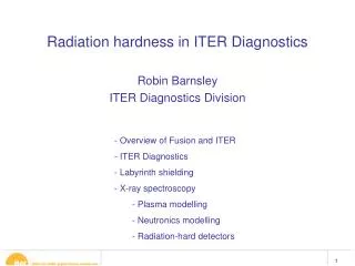
The ITER Project • ITER is a joint international R&D project that aims to demonstrate scientific and technical feasibility of fusion power. • ITER Partners are China, India, E.U., Japan, Korea, Russian Federation, and U.S.A. Tokamak Complex building ITER site in Cadarache
The ITER Tokamak Poloidal field coils Central Solenoid Toroidal field coils Plasma chamber Vacuum Vessel Cryostat Upper, equatorial, and lower ports
ITER Tokamak Building Bioshield Technical galleries
Radiation Hardness Assurance • Radiation constraints in ITER – preliminary figures • During operation, outside the vacuum vessel, the simulated dose rate is around 2.5 mGy/s. Assuming that the lethal dose for standard electronics is ~100 Gy, this corresponds to ~ 100 shots of 400 seconds each. • During maintenance, outside the vacuum vessel, the simulated dose rate can be as high as 3 mGy/h. This corresponds to 100 Gy in 3.8 years. • During maintenance, inside the vacuum vessel, the simulated level is several hundred Gy/h, well above the lethal dose of standard electronics. • The ITER approach • ITER is currently developing a policy inspired from the ATLAS approach. • This policy will apply to any electronics exposed to radiation in ITER, including « visible » electronics (crates, etc.) and « hidden » electronics (in electromechanical systems such as motors, etc). • As for ATLAS, this policy should be coherent, based on recognized test methods, efficient and cost effective. • Once developed, the implementation of this policy will require a substantial learning period in the ITER community.