Download
1 / 33
330 likes | 414 Vues
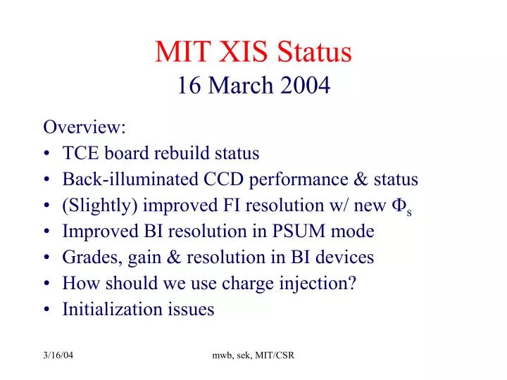
MIT XIS Status 16 March 2004. Overview: TCE board rebuild status Back-illuminated CCD performance & status (Slightly) improved FI resolution w/ new s Improved BI resolution in PSUM mode Grades, gain & resolution in BI devices How should we use charge injection? Initialization issues.

E N D
MIT XIS Status16 March 2004 Overview: • TCE board rebuild status • Back-illuminated CCD performance & status • (Slightly) improved FI resolution w/ new s • Improved BI resolution in PSUM mode • Grades, gain & resolution in BI devices • How should we use charge injection? • Initialization issues mwb, sek, MIT/CSR
Thermal Control Electronics Board Status • Four (revised) flight boards passed acceptance level vibration & thermal tests at MIT • Boards hand-carried to ISAS today • TCE board engineering test script defined, sent to Japan • Plan to install & test boards in flight AE/TCE in Osaka next week • Plan workmanship shake at ISAS (April?) mwb, sek, MIT/CSR
Back-illuminated CCD Progress • At November XIS team meeting we reported results from first chemisorption-charging XIS BI device. • Progress since then: • 4 more devices tested (5 total) from 2 wafers (1 CI wafer 1 non-CI wafer) • Revised clock voltages found (lower noise, no spurious charge) • Two devices calibrated (1 CI, one non-CI); QE model constrained • Charge injection function verified • 40 MeV proton irradiation to check radiation tolerance • Dark current, background rejection efficiency measured • >1000 hours total “CCD clocking” test time; ~50 thermal cycles • Flight sensor base with BI CCD built, passed vibration acceptance testing; thermal test in progress. • Generally, performance fulfills promise of first test results mwb, sek, MIT/CSR
Spectral Resolution & Quantum Efficiency Comparison: Back- & Front-illuminated XIS CCDs BI split threshold: 7e- 277 eV: QEBI/QEFI = 40.3 FWHMBI = 50-55 eV FWHMFI = 50-55 eV 525 eV: QEBI/QEFI = 3.3 FWHMBI = 60-65 eV FWHMFI = 45-50 eV mwb, sek, MIT/CSR
Measured XIS BI CCD Quantum Efficiency + BI Measurements BI QE Model Parameters mwb, sek, MIT/CSR
Chemisorption Charging ProcessBack Surface Structure 5 nm HfO2 1 nm Ag 3 nm SiO2 45 mm Si (not to scale) [ Deadlayer Sensitive Volume mwb, sek, MIT/CSR (Burke, Lesser et al., 2003)
XIS Effective Area Comparison: 1 BI Sensor vs 1 FI Sensor Includes XRT-I area & transmission of all filters mwb, sek, MIT/CSR
XIS Spectral Resolution: FI & BI CCDs mwb, sek, MIT/CSR
Back-illuminated Front-illuminated XIS Spectral Resolution Comparison: BI vs FI Simulated Spectra of SNR E0102 -72.3 OVIII OVII mwb, sek, MIT/CSR
BI CCD Spectral Resolution: XIS, Chandra ACIS & XMM-Newton EPIC-PN 10 Chandra ACIS-S 3.1 c s-1 Simulated Spectra of SNR E0102 -72.3 ct s-1 keV-1 10 XIS BI & FI 4.6 c s-1 (4 FI) 6.9 c s-1 (2 FI+2 BI) 1.5 0 20 ct s-1 keV-1 XMM-Newton EPIC-PN 8.0 c s-1 (EPN) 5.0 c s-1 (2EMOS) ct s-1 keV-1 0 1.5 Energy (keV) Note: EPIC MOS Resolution comparable to XIS (but is not a BI CCD) 0 1.5 Energy (keV) mwb, sek, MIT/CSR
XIS Dark Current Comparison: BI vs FI mwb, sek, MIT/CSR
Radiation Induced Pulse-height Shift in BI CCD Event Center Pixel Pulse-height (adu) Column Number mwb, sek, MIT/CSR
Radiation-Induced Loss of Spectral Resolution BI CCD at 5.9 keV FWHM at 5.9 keV (eV) Column Number mwb, sek, MIT/CSR
Radiation-Induced CTI Increase in XIS BI & FI CCDs mwb, sek, MIT/CSR
60Co Gamma/e- Response Comparison G02346 events • Background Rejection • Efficiency Comparison: • BI, FI similar @ E <1 keV • BI better 1-2.5 keV by x 2 • (mostly lower Si K fluorescence) • FI better 2.5-12 keV by x2.5 mwb, sek, MIT/CSR
BI Resolution in PSUM Mode mwb, sek, MIT/CSR
BI CCD Pulse-height vs Grade (390 eV) mwb, sek, MIT/CSR
BI CCD Pulse-height vs Grade Selection mwb, sek, MIT/CSR
BI Test Experience Summary • 5 BI devices tested from 2 wafers • >1000 hours total cold CCD-clocking time • > 50 thermal cycles (25 thermal cycles on one device) • Nominal calibration measurement suite run on 2 devices • Radiation testing (40 MeV protons) on one device • 60Co response checked • BI devices require slightly different clock levels • Flight-sensor base passed acceptance vibration; thermal test in progress. • No peculiar gain or QE instabilities noted to date. mwb, sek, MIT/CSR
Possible Additional BI ‘Stability’ Tests • UV (2600 A) flood test (at CSR): • Flood CCD with light from EEPROM burner • Look for gain/QE drift at low energies due to interface charging • Ly test (at Lincoln Lab): • Have ‘loaned’ one device to UV instrument team at LL • They will check response at Ly • This test will check deadlayer model • Extended high-temperature (+60C) aging test? • 2-day ‘informal’ test already done • Others? mwb, sek, MIT/CSR
Additional BI Calibration Needed • Additional QE data E< 0.5 keV • ‘Deadlayer is known only to 70 ± 20 nm • Additional data at 180 eV, 390 eV would be useful • Energy-scale data at E< 2 keV • Energy scale is not linear here • Spectral resolution with flight AE/TCE (all E) • BI resolution is quite sensitive to AE/TCE noise • Spatial QE non-uniformity at E> 6 keV • BI CCD seems to be slightly thinner than expected mwb, sek, MIT/CSR
XIS Sensor Base with Back-illuminated CCD • CCD calibrated at MIT • Vibration test passed 5 March • Thermal test in progress • Anticipate shipment 24 March mwb, sek, MIT/CSR
XIS BI Sensor Base Delivery Prospects • Anticipate 1st BI sensor base (with CCD w1.8c5) ready for shipment 24 March • Next flight candidate BI CCDs: • w1.8c2 now under test; CTI worse than w1.8c5 but could fly • w1.8c8 expected at CSR now • Third wafer still at University of Arizona • Engineering team has ISS commitments through April • CCD team (Bev) will calibrate 2nd flight BI device in April • Expect to deliver 2nd BI sensor base at end of May mwb, sek, MIT/CSR
FI Resolution & Noise with reduced Serial Clocks mwb, sek, MIT/CSR
How should we use charge injection? • Two possible uses: • CTI measurement (with checkered flag to allow ground correction) • CTI reduction (with grid to fill traps) • Tsuru-san finds poor correlation between injected amplitude & X-ray amplitude: • Very interesting & useful analysis; we had not done this! • Injected charge must be summed as events for stable injection (why?) • Inherent CTI in w1.3c6 is rather small (< 5 x 10⁻⁶) • I think there is hope for this method but I haven’t done my homework • So-called ‘grid’ method is very promising: • Improves resolution for radiation-damaged FI & BI chips • Loss of QE seems as expected (or better!) • How will DE handle injected grid? What about extra hot pixel rate? • Main questions: How & when do we decide about use of CI? mwb, sek, MIT/CSR
An Example: Injecting a Grid Pattern Charge moves right during injection Input Register ID/IG • Charge injection is programmable. • Purpose of “Grid” program is to reduce radiation damage effects: • Charge is injected in each column of every 54th row. • Injected charge (temporarily) fills radiation-induced traps. • Filled traps cannot contribute to charge transfer inefficiency. • Result is better spectral resolution. Charge moves down during readout Rows filled by charge injection
Effect of Proton Irradiation on XIS Response Without Charge Injection Prelaunch: FWHM: 132 eV. Post-irradiation (2 yr on-orbit equivalent): Gain shift 1.3%; FWHM: 210 eV
Effect of Proton Irradiation on XIS Response With Charge Injection Prelaunch: FWHM: 132 eV. Post-irradiation with charge injection: Gain shift 0.5%; FWHM: 144 eV
CTI at 5.9 keV vs Charge Injection Level Radiation-damaged BI CCD mwb, sek, MIT/CSR
Radiation-Induced Loss of Spectral Resolution in BI CCD FWHM at 5.9 keV (eV) Column Number mwb, sek, MIT/CSR
Resolution Improvement with Charge Injection Radiation-damaged BI CCD at 525 eV mwb, sek, MIT/CSR
Relative QE with Grid Charge Injection Radiation Damaged BI device • For quad B of BI w1.8c6 after 40 MeV proton irradation • Based on ‘counts under peak’; statistical precision ~0.005 • Injected charge rows treated as 0 in event finding * NB: 5.9 keV data do NOT have hot pixels removed mwb, sek, MIT/CSR