Download
1 / 16
160 likes | 318 Vues
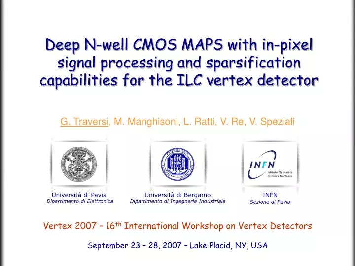
D eep N-well CMOS MAPS with in-pixel signal processing and sparsification capabilities for the ILC vertex detector. G. Traversi , M. Manghisoni , L. Ratti, V. Re, V. Speziali Vertex 200 7 – 16 th International Workshop on Vertex Detectors September 2 3 – 28 , 2007 – Lake Placid, NY, USA.

E N D
Deep N-well CMOS MAPS with in-pixel signal processing and sparsification capabilities for the ILC vertex detector G. Traversi, M. Manghisoni, L. Ratti, V. Re, V. Speziali Vertex 2007– 16th International Workshop on Vertex Detectors September 23 – 28, 2007 – Lake Placid, NY, USA Università di Pavia Dipartimento di Elettronica Università di Bergamo Dipartimento di Ingegneria Industriale INFN Sezione di Pavia
Outline Introduction: standard CMOS monolithic active pixel sensors Deep N-Well pixel sensor Description of the sensor level processor Digital section and digital readout scheme Physical simulations Conclusions 16th International Workshop on Vertex Detectors
Principle of operation: Signal generated by a particle is collected by an n-well/p-epitaxial diode, then readout by CMOS electronics integrated in the same substrate Charge generated by the incident particle moves by thermal diffusion Extremely simple in-pixel readout (3-T NMOS, PMOS not allowed) Several reasons make CMOS MAPS appealing as tracking devices: Electronics and interconnections Detector and readout on the same substrate Epi layer (~10um thick) Wafer can be thinned down to tens of mm minimal amount of material in the detector region (e.g. with respect to hybrid pixel) Substrate (~300um thick) Deep sub-micron CMOS tecnology high functional density and versatility, low power consumption, radiation tolerance and fabrication costs Conventional CMOS MAPS 16th International Workshop on Vertex Detectors
DNW MAPS is based on the same working principle as standard MAPS ADNW is used to collect the charge released in the epitaxial layer Acharge preamplifier is used for Q-V conversion gain decoupled from electrode capacitance DNW may houseNMOStransistors Using a large detector area, PMOS devices may be included in the front-end design charge collection inefficiency depending on the ratio of the DNW area to the area of all the N-wells (deep and standard) Deep Nwell sensor concept In triple-well CMOS processes a deep N-well is used to shield N-channel devices from substrate noise in mixed-signal circuits 16th International Workshop on Vertex Detectors
Sub. 2004 Sub. 2005 Sub. 2006 Sub. 2007 Sub. 2006 Sub. 2006 Sub. 2007 Sub. 2007 Sub. 2006 APSEL series chips SLIM5 Collaboration: INFN & Italian Universities Pisa, Pavia, Bergamo, Bologna, Trento, Trieste, Torino Full in-pixel signal processing: PA + shaper + comparator + latch Prototypes fabricated with the STMicroelectronics 130nm triple-well technology High sensitivity charge preamplifier with continuous reset + RC-CR shaper with programmable peaking time A threshold discriminator is used to drive a NOR latch featuring an external reset Pixel size about 50mm x 50mm The first prototypes proved the capability of the sensor to collect charge from the epitaxial layer 16th International Workshop on Vertex Detectors
bunch train interval intertrain interval Design specifications for the ILC vertex detector The beam structure of ILC will feature 2820crossingsin a 1 ms bunch train, with a duty-cycle of 0.5% assuming maximum hit occupancy 0.03part./Xing/mm2 if 3 pixels fire for every particlehitting hit rate 250 hits/train/mm2 if a digital readout is adopted 5mm resolution requires 17.3 mm pixel pitch 15 mm pitch Oc 0.056 hits/train 0.0016 probability of a pixel being hit at least twice in a bunch train period A pipeline with a depth of one in each cell should be sufficient to record > 99% of events without ambiguity Data can be readout in the intertrain interval system EMI insensitive 16th International Workshop on Vertex Detectors
In DNW MAPS sensors for ILC sparsification is based on a token passing readout scheme suggested by R. Yarema (R. Yarema, “Fermilab Initiatives in 3D Integrated Circuits and SOI Design for HEP”, ILC VTX Workshop at Ringberg, May 2006) Detection phase (corresponding to the bunch train interval) Readout phase (corresponding to the intertrain interval) MAPS sensor operation is tailored on the structure of ILC beam Sparsified readout architecture 16th International Workshop on Vertex Detectors
Preamplifier 22T 14T -G(s) CF Vt Discriminator iF Preamplifier response to an 800 e- pulse Pixel level processor CF obtained from the source-drain capacitance High frequency noise contribution has been reduced limiting the PA bandwidth ENC=25 e- rms@CD=100 fF Threshold dispersion 30 e- rms Power consumption 5 μW Features power-down capabilities for power saving: the analog section cell can be switched off during the intertrain interval in order to save power (1% duty-cycle seems feasible) 16th International Workshop on Vertex Detectors
Cell CK Cell digital section Includes a 5 bit time stamp register and the data sparsification logic Get X bus Get Y bus During the bunch train period, the hit latch is set in each hit pixel When the pixel is hit, the content of the time stamp register gets frozen 4T To the time stamp buffer Master Reset 76T t1 t2 t3 t4 t5 WE From the discriminator 10T 20T 13T OE hit S D Q getb_en Q OEb t1in t2in t3in t4in t5in hitb R CP Qb Qb Lat_en tokin CPb tokout time stamp register tokrst Get bus latch hit latch From the time stamp counter token passing core Cell CK 16th International Workshop on Vertex Detectors
analog front-end + • Preamplifier • Discriminator digital section 164 transistors DNW sensor 25 mm Sparsification logic Time stamp register 25 mm ILC DNW elementary cell 16th International Workshop on Vertex Detectors
Readout CK 4 X Readout phase: 4 Y MUX • token is sent 5 Serial data output T Cell CK 4 5 4 5 4 5 Time Stamp Buffer 1 Time Stamp Buffer 2 Time Stamp Buffer 16 X=1 X=2 X=16 • the pixel points to the • X and Y registers at • the periphery and 1 1 1 5 5 5 Cell (1,1) Cell (1,2) Cell (1,16) gXb gXb gXb gXb=get_X_bus gYb=get_Y_bus TS=Time_Stamp Tkin=token_in Tkout=Token_out • sends off the time • stamp register content First token in TS TS TS Tkin Tkout Tkin Tkout Tkin Tkout • data are serialized and • token scans ahaed 4 1 gYb gYb gYb Y=1 Cell (2,1) Cell (2,2) Cell (2,16) gXb gXb gXb TS TS TS Tkout Tkin Tkout Tkin Tkout Tkin 4 1 gYb gYb gYb The number of elements may be increased without changing the pixel logic (just larger X- and Y-registers and serializer will be required) Y=2 Cell (16,1) Cell (16,2) Cell (16,16) gXb gXb gXb Last token out TS TS TS Tkout Tkin Tkout Tkin Tkout Tkin 4 1 gYb gYb gYb Y=16 Digital readout scheme • token scans the matrix and • gets caught by the first • hit pixel Hit pixel 16th International Workshop on Vertex Detectors
Because low material budget is necessary, there is little room for cooling system very low power operation Analog power: Pan,pix 5mW/pixel (dissipated in the analog PA) Digital power: PDC,pix 7 nW/pixel (leakage currents of the digital blocks) Pdyn,pix 20 nW/pixel (to charge the input capacitance of the time stamp register blocks during the detection phase) (power in the periphery neglected since it grows as the square root of the number of matrix cells) 15.5 W 13.6 W 1.9 W 0.05 W Assuming: - 170000mm2 total vertex detector area (pixel pitch of 25 mm); - 1 Mpixel chips; - dP=0.01 power supply duty cycle N= number of cell per pixel M= number of chip composing the detector Power dissipation analysis 16th International Workshop on Vertex Detectors
Standard N-well TCAD simulations Deep N-well collecting electrode Monte Carlo simulations Charge collected by the central pixel in the 3×3 SDR0 matrix Physical simulation performed by E. Pozzati - University of Pavia (Italy) 3D device simulations • The simulated structure (with TCAD) required a mesh with 165000 vertices. Because of the really long computation time only 36 simulations, each involving a different MIP collision point, have been performed • MAPS operation is mainly diffusiondriven computing power required by TCAD may not be needed • Monte Carlo code based on random walk developed (results of a collaboration with D. Christian – Fermilab) • Activity presently focused on finely tuning a three-dimensional diffusion modelfor Monte Carlo simulations of MAPS by comparison with TCAD simulation results • Advantage: dramatic reduction in computing time • Next step: take advantage of fast Monte Carlo simulator to maximize detection efficiency through suitable layout choice 16th International Workshop on Vertex Detectors
Delivered end of July 2007 The chip includes: a 16 by 16 MAPS matrix (25μm pitch) with digital sparsified readout an 8 by 8 MAPS matrix (25μm pitch) with digital sparsified readout and selectable access to the output of the PA in each cell a 3 by 3 MAPS matrix (25μm pitch) with all of the PA output accessible at the same time 3 standalone readout channels with different CD (detector simulating capacitance) The demonstrator chip (SDR0) 8 x 8 matrix 16 x 16 matrix Single pixel test structures 3 x 3 matrix 16th International Workshop on Vertex Detectors
The SDR0 test board Credit: Fabio Risigo University of Insubria, Como (Italy) Test board designed by Marcin JastrzabUniversity of Science and Technology, Cracow (Poland) and University of Insubria, Como (Italy) 16th International Workshop on Vertex Detectors
Conclusions New DNW MAPS structures with optimized noise and threshold dispersion characteristics have been fabricated in the 130 nm, triple well STM CMOS technology Study of the charge collection efficiency and of charge spreading in the epi-layer is underway to assess their suitability for tracking and vertexing applications Monte Carlo method will be used, besides Synopsys TCAD software package, in the design of the next generation prototype chips Characterization of a DNW MAPS demonstrator aimed at vertexing applications at the ILC is foregoing Plans for the future: design of a 256 x 256 matrix for beam test evaluation of more scaled technologies (90 nm CMOS) 16th International Workshop on Vertex Detectors