Download
1 / 32
390 likes | 620 Vues
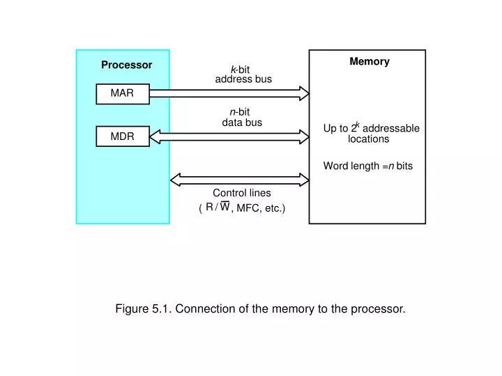
Memory. Processor. k. -bit. address bus. MAR. n. -bit. data bus. k. Up to 2. addressable. MDR. locations. Word length =. n. bits. Control lines. R. /. W. ( , MFC, etc.). Figure 5.1. Connection of the memory to the processor. b. b. ¢. b. b. ¢. b. b. ¢. 7.

E N D
Memory Processor k -bit address bus MAR n -bit data bus k Up to 2 addressable MDR locations Word length = n bits Control lines R / W ( , MFC, etc.) Figure 5.1.Connection of the memory to the processor.
b b ¢ b b ¢ b b ¢ 7 7 1 1 0 0 • • • W 0 FF FF A • • • 0 W 1 A 1 Address Memory • • • • • • • • • • • • • • • • • • cells decoder A 2 A 3 • • • W 15 R / W Sense / Write Sense / Write Sense / Write circuit circuit circuit CS Data input /output lines: b b b 7 1 0 Figure 5.2.Organization of bit cells in a memory chip.
5-bit row address W 0 W 1 32 ´ 32 5-bit memory cell decoder array W 31 Sense / Write circuitry 10-bit address 32-to-1 R / W output multiplexer and CS input demultiplexer 5-bit column address Data input/output Figure 5.3. Organization of a 1K 1 memory chip.
b b ¢ T T 1 2 X Y Word line Bit lines Figure 5.4. A static RAM cell.
Bit line Word line T C Figure 5.6.A single-transistor dynamic memory cell
R A S Row Row 4096 ´ ( 512 ´ 8 ) address decoder cell array latch A ¤ A CS Sense / Write 20 - 9 8 - 0 circuits R / W Column Column address decoder latch C A S D D 7 0 Figure 5.7. Internal organization of a 2M ´ 8 dynamic memory chip.
Refresh counter Row Ro w address Cell array decoder latch Row/Column address Column Co lumn Read/Write address circuits & latches decoder counter Clock R A S Mode register Data input Data output C A S and register register timing control R / W C S Data Figure 5.8.Synchronous DRAM.
Clock R / W R A S C A S Address Row Col Data D0 D1 D2 D3 Figure 5.9.Burst read of length 4 in an SDRAM.
21-bit addresses 19-bit internal chip address A 0 A 1 A 19 A 20 2-bit decoder 512 K ´ 8 memory chip D D D D 31-24 23-16 15-8 7-0 512 K ´ 8 memory chip 19-bit 8-bit data address input/output Chip select Figure 5.10. Organization of a 2M 32 memory module using 512K 8 static memory chips.
Row/Column address Address R A S R / W C A S Memory controller Request R / W Processor Memory C S Clock Clock Data Figure 5.11. Use of a memory controller.
Not connected to store a 1 Connected to store a 0 Bit line Word line T P Figure 5.12.A ROM cell.
Pr ocessor Re gisters Increasing Increasing Increasing size speed cost per bit Primary L1 cache Secondary L2 cache Main memory Magnetic disk secondary memory Figure 5.13.Memory hierarchy.
Main Processor Cache memory Figure 5.14.Use of a cache memory.
Please see “portrait orientation” PowerPoint file for Chapter 5 Figure 5.15. Direct-mapped cache.
Please see “portrait orientation” PowerPoint file for Chapter 5 Figure 5.16. Associative-mapped cache.
Please see “portrait orientation” PowerPoint file for Chapter 5 Figure 5.17. Set-associative-mapped cache with two blocks per set.
Memory address Contents A(0,0) 0 1 1 1 1 0 1 0 0 0 0 0 0 0 0 0 A(1,0) 0 1 1 1 1 0 1 0 0 0 0 0 0 0 0 1 0 1 1 1 1 0 1 0 0 0 0 0 0 0 1 0 A(2,0) 0 1 1 1 1 0 1 0 0 0 0 0 0 0 1 1 A(3,0) A(0,1) 0 1 1 1 1 0 1 0 0 0 0 0 0 1 0 0 0 1 1 1 1 0 1 0 0 0 1 0 0 1 0 0 A(0,9) 0 1 1 1 1 0 1 0 0 0 1 0 0 1 0 1 A(1,9) 0 1 1 1 1 0 1 0 0 0 1 0 0 1 1 0 A(2,9) A(3,9) 0 1 1 1 1 0 1 0 0 0 1 0 0 1 1 1 T ag for direct mapped T ag for set-associati v e T ag for associati v e (7A00) (7A01) (7A02) (7A03) (7A04) (7A24) (7A25) (7A26) (7A27) Figure 5.18.An array stored in the main memory.
SUM := 0 j:= 0 9 for to do SUM := SUM + A(0,j) end A VE := SUM / 10 for i:= 9 0 do wn to do A(0,i) := A(0,i) / A VE end Figure 5.19. Task for example in Section 5.5.3.
Contents of data cache after pass: Block j = 1 j = 3 j = 5 j = 7 j = 9 i = 6 i = 4 i = 2 i = 0 position 0 A(0,0) A(0,2) A(0,4) A(0,6) A(0,8) A(0,6) A(0,4) A(0,2) A(0,0) 1 2 3 4 A(0,1) A(0,3) A(0,5) A(0,7) A(0,9) A(0,7) A(0,5) A(0,3) A(0,1) 5 6 7 Figure 5.20.Contents of a direct-mapped data cache in Example 5.1.
Contents of data cache after pass: Block j = 7 j = 8 j = 9 i = 1 i = 0 position 0 A(0,0) A(0,8) A(0,8) A(0,8) A(0,0) A(0,1) A(0,1) A(0,9) A(0,1) A(0,1) 1 2 A(0,2) A(0,2) A(0,2) A(0,2) A(0,2) A(0,3) A(0,3) A(0,3) A(0,3) A(0,3) 3 4 A(0,4) A(0,4) A(0,4) A(0,4) A(0,4) A(0,5) A(0,5) A(0,5) A(0,5) A(0,5) 5 6 A(0,6) A(0,6) A(0,6) A(0,6) A(0,6) A(0,7) A(0,7) A(0,7) A(0,7) A(0,7) 7 Figure 5.21. Contents of an associative-mapped data cache in Example 5.1.
Contents of data cache after pass: j = 3 j = 7 j = 9 i = 4 i = 2 i = 0 A(0,0) A(0,4) A(0,8) A(0,4) A(0,4) A(0,0) A(0,1) A(0,5) A(0,9) A(0,5) A(0,5) A(0,1) Set 0 A(0,2) A(0,6) A(0,6) A(0,6) A(0,2) A(0,2) A(0,3) A(0,7) A(0,7) A(0,7) A(0,3) A(0,3) Set 1 Figure 5.22. Contents of a set-associative-mapped data cache in Example 5.1.
Please see “portrait orientation” PowerPoint file for Chapter 5 Figure 5.23. Data cache organization in 68040 microprocessor.
Processing units L1 instruction L1 data cache cache Bus interface unit System bus Cache bus Main L2 cache Input/Output memory Figure 5.24. Caches and external connections in Pentium III processor.
Please see “portrait orientation” PowerPoint file for Chapter 5 Figure 5.25. Addressing multiple-module memory systems.
Please see “portrait orientation” PowerPoint file for Chapter 5 Figure 5.27. Virtual-memory address translation.
Please see “portrait orientation” PowerPoint file for Chapter 5 Figure 5.28. Use of an associative-mapped TLB.
Sector 0, track 1 Sector 3, track n Sector 0, track 0 Figure 5.30. Organization of one surface of a disk.
Processor Main memory System bus Disk controller Disk drive Disk drive Figure 5.31. Disks connected to the system bus.
Please see “portrait orientation” PowerPoint file for Chapter 5 Figure 5.32. Optical disk.
File File mark File mark 7 or 9 • • • • • • • • bits File gap Record Record Record Record gap gap Figure 5.33. Organization of data on magnetic tape.