Download
1 / 221
2.26k likes | 2.63k Vues
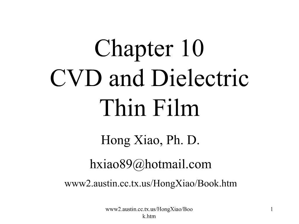
Hong Xiao, Ph. D.. www2.austin.cc.tx.us/HongXiao/Book.htm. 2. Objectives. Identify at least four CVD applicationsDescribe CVD process sequenceList the two deposition regimes and describe their relation to temperatureList two dielectric thin filmsName the two most commonly used silicon precursors

E N D
1. Hong Xiao, Ph. D. www2.austin.cc.tx.us/HongXiao/Book.htm 1
2. Hong Xiao, Ph. D. www2.austin.cc.tx.us/HongXiao/Book.htm 2 Objectives Identify at least four CVD applications
Describe CVD process sequence
List the two deposition regimes and describe their relation to temperature
List two dielectric thin films
Name the two most commonly used silicon precursors for dielectric CVD
3. Hong Xiao, Ph. D. www2.austin.cc.tx.us/HongXiao/Book.htm 3 CVD Oxide vs. Grown Oxide
4. Hong Xiao, Ph. D. www2.austin.cc.tx.us/HongXiao/Book.htm 4 CVD Oxide vs. Grown Oxide
5. Hong Xiao, Ph. D. www2.austin.cc.tx.us/HongXiao/Book.htm 5 Dielectric Thin Film Applications Multi-level metal interconnection
CVD and SOG plus CVD dielectrics
Shallow trench isolation (STI)
Sidewall spacer for salicide, LDD, and the source/drain diffusion buffer
The passivation dielectric (PD)
Dielectric ARC for feature size < 0.25 mm
6. Hong Xiao, Ph. D. www2.austin.cc.tx.us/HongXiao/Book.htm 6 Dielectric Thin Film Applications Inter layer dielectric, or ILD, include PMD and IMD
Pre-metal dielectric: PMD
normally PSG or BPSG
Temperature limited by thermal budget
Inter-metal dielectric: IMD
USG or FSG
Normally deposited around 400 ?C
7. Hong Xiao, Ph. D. www2.austin.cc.tx.us/HongXiao/Book.htm 7
8. Hong Xiao, Ph. D. www2.austin.cc.tx.us/HongXiao/Book.htm 8 Dielectric Processes
9. Hong Xiao, Ph. D. www2.austin.cc.tx.us/HongXiao/Book.htm 9 CVD
10. Hong Xiao, Ph. D. www2.austin.cc.tx.us/HongXiao/Book.htm 10 CVD Applications
11. Hong Xiao, Ph. D. www2.austin.cc.tx.us/HongXiao/Book.htm 11 CVD
12. Hong Xiao, Ph. D. www2.austin.cc.tx.us/HongXiao/Book.htm 12 Figure 10.3
13. Hong Xiao, Ph. D. www2.austin.cc.tx.us/HongXiao/Book.htm 13 Deposition Process
14. Hong Xiao, Ph. D. www2.austin.cc.tx.us/HongXiao/Book.htm 14 Deposition Process
15. Hong Xiao, Ph. D. www2.austin.cc.tx.us/HongXiao/Book.htm 15 CVD Processes APCVD
LPCVD
PECVD
16. Hong Xiao, Ph. D. www2.austin.cc.tx.us/HongXiao/Book.htm 16
17. Hong Xiao, Ph. D. www2.austin.cc.tx.us/HongXiao/Book.htm 17
18. Hong Xiao, Ph. D. www2.austin.cc.tx.us/HongXiao/Book.htm 18 Question A semiconductor manufacturer has its R&D lab on the coast near sea level and one of its manufacturing fabs on a high altitude plateau. It was found that the APCVD processes developed in the R&D lab couldn�t directly apply in that particular fab. Why?
19. Hong Xiao, Ph. D. www2.austin.cc.tx.us/HongXiao/Book.htm 19 Answer On a high-altitude plateau, the atmospheric pressure is significantly lower than at sea level. Because earlier APCVD reactor didn�t have a pressure-control system, a process that worked fine in the R&D lab at sea level might not work well in the high altitude fab because of pressure difference
20. Hong Xiao, Ph. D. www2.austin.cc.tx.us/HongXiao/Book.htm 20
21. Hong Xiao, Ph. D. www2.austin.cc.tx.us/HongXiao/Book.htm 21
22. Hong Xiao, Ph. D. www2.austin.cc.tx.us/HongXiao/Book.htm 22 LPCVD System
23. Hong Xiao, Ph. D. www2.austin.cc.tx.us/HongXiao/Book.htm 23 PECVD
24. Hong Xiao, Ph. D. www2.austin.cc.tx.us/HongXiao/Book.htm 24
25. Hong Xiao, Ph. D. www2.austin.cc.tx.us/HongXiao/Book.htm 25 Step Coverage A measurement of the deposited film reproducing the slope of a step on the substrate surface
One of the most important specifications
Sidewall step coverage
Bottom step coverage
Conformality
Overhang
26. Hong Xiao, Ph. D. www2.austin.cc.tx.us/HongXiao/Book.htm 26 Step Coverage and Conformity
27. Hong Xiao, Ph. D. www2.austin.cc.tx.us/HongXiao/Book.htm 27 Factors Affect Step Coverage Arriving angle of precursor
Surface mobility of adsorbed precursor
28. Hong Xiao, Ph. D. www2.austin.cc.tx.us/HongXiao/Book.htm 28 Arriving Angles
29. Hong Xiao, Ph. D. www2.austin.cc.tx.us/HongXiao/Book.htm 29 Arriving Angle Corner A: 270?, corner C: 90?
More precursors at corner A
More deposition
Form the overhang
Overhang can cause voids or keyholes
30. Hong Xiao, Ph. D. www2.austin.cc.tx.us/HongXiao/Book.htm 30 Void Formation Process
31. Hong Xiao, Ph. D. www2.austin.cc.tx.us/HongXiao/Book.htm 31 Control of Arriving Angle |Changing pressure
Tapering opening
32. Hong Xiao, Ph. D. www2.austin.cc.tx.us/HongXiao/Book.htm 32 Step Coverage, Pressure and Surface Mobility
33. Hong Xiao, Ph. D. www2.austin.cc.tx.us/HongXiao/Book.htm 33 Arriving Angles, Contact Holes
34. Hong Xiao, Ph. D. www2.austin.cc.tx.us/HongXiao/Book.htm 34 Gap Fill Fill a gap without voids
Voids: cause defect and reliability problems
Deposition/Etchback/Deposition
Silane and PE-TEOS film
Conformal deposition
O3-TEOS and tungsten CVD
High density plasma CVD
35. Hong Xiao, Ph. D. www2.austin.cc.tx.us/HongXiao/Book.htm 35 Gap Fill PMD: zero tolerance voids
Tungsten can be deposited into these voids
Causing shorts
IMD: voids below metal may tolerable
reducing k
process gas could come out later and cause reliability problem
36. Hong Xiao, Ph. D. www2.austin.cc.tx.us/HongXiao/Book.htm 36 Void in PMD
37. Hong Xiao, Ph. D. www2.austin.cc.tx.us/HongXiao/Book.htm 37 Unwanted W Line Between Gates
38. Hong Xiao, Ph. D. www2.austin.cc.tx.us/HongXiao/Book.htm 38 Deposition/Etchback/Deposition
39. Hong Xiao, Ph. D. www2.austin.cc.tx.us/HongXiao/Book.htm 39 Conformal Deposition Gap Fill
40. Hong Xiao, Ph. D. www2.austin.cc.tx.us/HongXiao/Book.htm 40 Conformal Deposition Gap Fill
41. Hong Xiao, Ph. D. www2.austin.cc.tx.us/HongXiao/Book.htm 41 Conformal Deposition Gap Fill
42. Hong Xiao, Ph. D. www2.austin.cc.tx.us/HongXiao/Book.htm 42
43. Hong Xiao, Ph. D. www2.austin.cc.tx.us/HongXiao/Book.htm 43 Surface Adsorption Determine precursors surface mobility
Affect step coverage and gap fill
Physical adsorption (physisorption)
Chemical adsorption (chemisorption)
44. Hong Xiao, Ph. D. www2.austin.cc.tx.us/HongXiao/Book.htm 44 Chemisorption Actual chemical bonds between surface atom and the adsorbed precursor molecule
Bonding energy usually exceeding 2 eV
Low surface mobility
Ion bombardment with10 to 20 eV energy in PECVD processes can cause some surface migration of chemisorbed precursors
45. Hong Xiao, Ph. D. www2.austin.cc.tx.us/HongXiao/Book.htm 45 Physisorption Weak bond between surface and precursor
Bonding energy usually less than 0.5 eV
Hydrogen bonding
Van der Waals forces
Ion bombardment and thermal energy at 400 ?C can cause migration of physisorbed precursors
High surface mobility
46. Hong Xiao, Ph. D. www2.austin.cc.tx.us/HongXiao/Book.htm 46
47. Hong Xiao, Ph. D. www2.austin.cc.tx.us/HongXiao/Book.htm 47 Dielectric CVD Precursors Silane (SiH4)
TEOS (tetra-ethyl-oxy-silane, Si(OC2H5)4)
48. Hong Xiao, Ph. D. www2.austin.cc.tx.us/HongXiao/Book.htm 48 CVD Precursor: Silane Dielectric CVD
PECVD passivation dielectric depositions
PMD barrier nitride layer
Dielectric anti reflective coating (DARC)
High density plasma CVD oxide processes
LPCVD poly-Si and silicon nitride
Metal CVD
W CVD process for nucleation step
Silicon source for WSix deposition
49. Hong Xiao, Ph. D. www2.austin.cc.tx.us/HongXiao/Book.htm 49 Dielectric CVD Precursor: Silane Pyrophoric (ignite itself), explosive, and toxic
Open silane line without thoroughly purging can cause fire or minor explosion and dust line
50. Hong Xiao, Ph. D. www2.austin.cc.tx.us/HongXiao/Book.htm 50
51. Hong Xiao, Ph. D. www2.austin.cc.tx.us/HongXiao/Book.htm 51 CVD Precursor Adsorption: Silane Silane molecule is perfectly symmetrical
Neither chemisorb nor physisorb
Fragments of silane, SiH3, SiH2, or SiH, can easily form chemical bonds with surface
Low surface mobility, overhangs and poor step coverage
52. Hong Xiao, Ph. D. www2.austin.cc.tx.us/HongXiao/Book.htm 52 CVD Precursor Adsorption: TEOS TEOS (tetra-ethyl-oxy-silane, Si(OC2H5)4)
Big organic molecule
TEOS molecule is not perfectly symmetric
Can form hydrogen bond and physisorb
High surface mobility
Good step coverage, conformality, and gap fill
Widely used for oxide deposition
53. Hong Xiao, Ph. D. www2.austin.cc.tx.us/HongXiao/Book.htm 53
54. Hong Xiao, Ph. D. www2.austin.cc.tx.us/HongXiao/Book.htm 54 TEOS Applications STI, sidewall spacer, PMD, and IMD
Most dielectric CVD processes are TEOS based oxide processes
55. Hong Xiao, Ph. D. www2.austin.cc.tx.us/HongXiao/Book.htm 55
56. Hong Xiao, Ph. D. www2.austin.cc.tx.us/HongXiao/Book.htm 56 TEOS Delivery A liquid at room temperature with boiling point at the sea level is 168 ?C
As a reference, boiling point of water (H2O) at sea level is 100 ?C
Need delivery system to send its vapor to process chamber
Boiler, bubbler, and injection systems
57. Hong Xiao, Ph. D. www2.austin.cc.tx.us/HongXiao/Book.htm 57
58. Hong Xiao, Ph. D. www2.austin.cc.tx.us/HongXiao/Book.htm 58
59. Hong Xiao, Ph. D. www2.austin.cc.tx.us/HongXiao/Book.htm 59
60. Hong Xiao, Ph. D. www2.austin.cc.tx.us/HongXiao/Book.htm 60 Sticking Coefficient The probability that precursor atom forms chemical bond with surface atom in one collision
Can be calculated by comparing the calculated deposition rate with 100% sticking coefficient and the measured actual deposition rate
61. Hong Xiao, Ph. D. www2.austin.cc.tx.us/HongXiao/Book.htm 61 Sticking Coefficient
62. Hong Xiao, Ph. D. www2.austin.cc.tx.us/HongXiao/Book.htm 62
63. Hong Xiao, Ph. D. www2.austin.cc.tx.us/HongXiao/Book.htm 63 Question Why don�t people apply TEOS as the silicon source gas for the silicon nitride deposition to get better step coverage for the nitride film
64. Hong Xiao, Ph. D. www2.austin.cc.tx.us/HongXiao/Book.htm 64 Answer In the TEOS molecule, the silicon atom is bonded with four oxygen atoms. It is almost impossible to strip all oxygen atoms and have silicon bonded only with nitrogen. Therefore, TEOS is mainly used for the oxide deposition and the nitride deposition normally uses silane as the silicon source gas
65. Hong Xiao, Ph. D. www2.austin.cc.tx.us/HongXiao/Book.htm 65 Chemical Reaction Rate
66. Hong Xiao, Ph. D. www2.austin.cc.tx.us/HongXiao/Book.htm 66 Deposition Regimes
67. Hong Xiao, Ph. D. www2.austin.cc.tx.us/HongXiao/Book.htm 67 Surface-Reaction-Limited Regime Chemical reaction rate can�t match precursor diffusion and adsorption rates; precursors pile up on the substrate surface and wait their turn to react.
D.R. = C.R. [B] [C] []�
Deposition rate is very sensitive to temperature
68. Hong Xiao, Ph. D. www2.austin.cc.tx.us/HongXiao/Book.htm 68 Mass-Transport-Limited Regime When the surface chemical reaction rate is high enough, the chemical precursors react immediately when they adsorb on the substrate surface.
Deposition rate = D dn/dx [B] [C] []�
Deposition rate is insensitive to temperature
Mainly controlled by gas flow rates
69. Hong Xiao, Ph. D. www2.austin.cc.tx.us/HongXiao/Book.htm 69 Deposition Rage Regimes
70. Hong Xiao, Ph. D. www2.austin.cc.tx.us/HongXiao/Book.htm 70 CVD Reactor Deposition Regime Most single wafer process reactors are designed in mass-transport-limited regime
It is easier to control the gas flow rate
Plasma or unstable chemicals such as ozone are used to achieve mass-transport-limited-regime at relatively low temperature
71. Hong Xiao, Ph. D. www2.austin.cc.tx.us/HongXiao/Book.htm 71 Applications of Dielectric Thin film
72. Hong Xiao, Ph. D. www2.austin.cc.tx.us/HongXiao/Book.htm 72 Dielectric CVD, Oxide and Nitride
73. Hong Xiao, Ph. D. www2.austin.cc.tx.us/HongXiao/Book.htm 73 Shallow Trench Isolation (STI)
74. Hong Xiao, Ph. D. www2.austin.cc.tx.us/HongXiao/Book.htm 74 Shallow Trench Isolation (STI)
75. Hong Xiao, Ph. D. www2.austin.cc.tx.us/HongXiao/Book.htm 75 Sidewall Spacer Formation
76. Hong Xiao, Ph. D. www2.austin.cc.tx.us/HongXiao/Book.htm 76 PMD
77. Hong Xiao, Ph. D. www2.austin.cc.tx.us/HongXiao/Book.htm 77 Sodium Ion Turn-on the MOSFET
78. Hong Xiao, Ph. D. www2.austin.cc.tx.us/HongXiao/Book.htm 78 PMD
79. Hong Xiao, Ph. D. www2.austin.cc.tx.us/HongXiao/Book.htm 79 Question Silicon nitride is a better sodium barrier layer than silicon oxide. Why don�t people just use nitride for PMD layer?
80. Hong Xiao, Ph. D. www2.austin.cc.tx.us/HongXiao/Book.htm 80 Answer Silicon nitride has higher dielectric constant
Using nitride can cause longer RC time delay and reduce circuit speed
A thin layer of nitride (~ 200 �) is commonly used as a diffusion barrier layer in the PMD application
Prevent diffusion of phosphorus and boron from BPSG diffusing into source/drain
81. Hong Xiao, Ph. D. www2.austin.cc.tx.us/HongXiao/Book.htm 81 PSG Reflow at 1100 �C, N2, 20 min.
82. Hong Xiao, Ph. D. www2.austin.cc.tx.us/HongXiao/Book.htm 82 Some Facts about Sodium
83. Hong Xiao, Ph. D. www2.austin.cc.tx.us/HongXiao/Book.htm 83 4?4 BPSG Reflow at 850 ?C, 30 Minutes in N2 Ambient
84. Hong Xiao, Ph. D. www2.austin.cc.tx.us/HongXiao/Book.htm 84 Development of PMD Processes
85. Hong Xiao, Ph. D. www2.austin.cc.tx.us/HongXiao/Book.htm 85
86. Hong Xiao, Ph. D. www2.austin.cc.tx.us/HongXiao/Book.htm 86 IMD
87. Hong Xiao, Ph. D. www2.austin.cc.tx.us/HongXiao/Book.htm 87 TEOS
88. Hong Xiao, Ph. D. www2.austin.cc.tx.us/HongXiao/Book.htm 88 PE-TEOS
89. Hong Xiao, Ph. D. www2.austin.cc.tx.us/HongXiao/Book.htm 89
90. Hong Xiao, Ph. D. www2.austin.cc.tx.us/HongXiao/Book.htm 90 PE-TEOS
91. Hong Xiao, Ph. D. www2.austin.cc.tx.us/HongXiao/Book.htm 91 O3-TEOS
92. Hong Xiao, Ph. D. www2.austin.cc.tx.us/HongXiao/Book.htm 92 O3-TEOS vs PE-TEOS
93. Hong Xiao, Ph. D. www2.austin.cc.tx.us/HongXiao/Book.htm 93 High Density Plasma CVD
94. Hong Xiao, Ph. D. www2.austin.cc.tx.us/HongXiao/Book.htm 94
95. Hong Xiao, Ph. D. www2.austin.cc.tx.us/HongXiao/Book.htm 95
96. Hong Xiao, Ph. D. www2.austin.cc.tx.us/HongXiao/Book.htm 96 Passivation
97. Hong Xiao, Ph. D. www2.austin.cc.tx.us/HongXiao/Book.htm 97 Dielectric Thin Film Characteristics Refractive index
Thickness
Uniformity
Stress
Particles
98. Hong Xiao, Ph. D. www2.austin.cc.tx.us/HongXiao/Book.htm 98 Refractive Index
99. Hong Xiao, Ph. D. www2.austin.cc.tx.us/HongXiao/Book.htm 99
100. Hong Xiao, Ph. D. www2.austin.cc.tx.us/HongXiao/Book.htm 100
101. Hong Xiao, Ph. D. www2.austin.cc.tx.us/HongXiao/Book.htm 101
102. Hong Xiao, Ph. D. www2.austin.cc.tx.us/HongXiao/Book.htm 102
103. Hong Xiao, Ph. D. www2.austin.cc.tx.us/HongXiao/Book.htm 103
104. Hong Xiao, Ph. D. www2.austin.cc.tx.us/HongXiao/Book.htm 104
105. Hong Xiao, Ph. D. www2.austin.cc.tx.us/HongXiao/Book.htm 105 Comparison of the Two Methods Ellipsometry
Need know rough film thickness before hand
Can measure thickness if R.I. is know
106. Hong Xiao, Ph. D. www2.austin.cc.tx.us/HongXiao/Book.htm 106 Thickness Measurement One of the most important measurements for dielectric thin film processes.
Determines
Film deposition rate
Wet etch rate
Shrinkage
107. Hong Xiao, Ph. D. www2.austin.cc.tx.us/HongXiao/Book.htm 107 Dielectric Thin Film Thickness Measurement
108. Hong Xiao, Ph. D. www2.austin.cc.tx.us/HongXiao/Book.htm 108 Dielectric Thin Film Thickness Measurement
109. Hong Xiao, Ph. D. www2.austin.cc.tx.us/HongXiao/Book.htm 109 Question
110. Hong Xiao, Ph. D. www2.austin.cc.tx.us/HongXiao/Book.htm 110 Answer
111. Hong Xiao, Ph. D. www2.austin.cc.tx.us/HongXiao/Book.htm 111 Question
112. Hong Xiao, Ph. D. www2.austin.cc.tx.us/HongXiao/Book.htm 112 Answer
113. Hong Xiao, Ph. D. www2.austin.cc.tx.us/HongXiao/Book.htm 113 Spectroreflectometry
114. Hong Xiao, Ph. D. www2.austin.cc.tx.us/HongXiao/Book.htm 114
115. Hong Xiao, Ph. D. www2.austin.cc.tx.us/HongXiao/Book.htm 115 Spectroreflectometry System
116. Hong Xiao, Ph. D. www2.austin.cc.tx.us/HongXiao/Book.htm 116 Question Many advance thin film thickness measurement tools allows user to choose the refractive index of the film. If someone mistakenly chooses the PE-TEOS USG film refractive index to measure O3-TEOS USG films thickness, what will be the effect on the measurement result?
117. Hong Xiao, Ph. D. www2.austin.cc.tx.us/HongXiao/Book.htm 117 Answer Since the nt always coupled together
A wrong n will cause wrong t measurement
O3-TEOS USG is a porous film and has a R.I., about 1.44
Slightly lower than 1.46 of PE-TEOS USG
Measured O3-TEOS film thickness will be slightly thinner than its actual value
118. Hong Xiao, Ph. D. www2.austin.cc.tx.us/HongXiao/Book.htm 118
119. Hong Xiao, Ph. D. www2.austin.cc.tx.us/HongXiao/Book.htm 119
120. Hong Xiao, Ph. D. www2.austin.cc.tx.us/HongXiao/Book.htm 120 Uniformity Multi-point measurement
Definition
Average:
Standard deviation:
Standard deviation non-uniformity: s/x
121. Hong Xiao, Ph. D. www2.austin.cc.tx.us/HongXiao/Book.htm 121 Stress Mismatch between different materials
Two kinds of stresses, intrinsic and extrinsic
Intrinsic stress develops during the film nucleation and growth process.
The extrinsic stress results from differences in the coefficients of thermal expansion
Tensile stress: cracking film if too high
Compressive stress: hillock if too strong
122. Hong Xiao, Ph. D. www2.austin.cc.tx.us/HongXiao/Book.htm 122
123. Hong Xiao, Ph. D. www2.austin.cc.tx.us/HongXiao/Book.htm 123 Illustration of Thermal Stress
124. Hong Xiao, Ph. D. www2.austin.cc.tx.us/HongXiao/Book.htm 124 Coefficients of Thermal Expansion
125. Hong Xiao, Ph. D. www2.austin.cc.tx.us/HongXiao/Book.htm 125 Stress Measurement
126. Hong Xiao, Ph. D. www2.austin.cc.tx.us/HongXiao/Book.htm 126
127. Hong Xiao, Ph. D. www2.austin.cc.tx.us/HongXiao/Book.htm 127 Dielectric CVD Processes Thermal Silane CVD Process
Thermal TEOS CVD Process
PECVD Silane Processes
PECVD TEOS Processes
Dielectric Etchback Processes
O3-TEOS Processes
Spin-on Glass
High Density Plasma CVD
128. Hong Xiao, Ph. D. www2.austin.cc.tx.us/HongXiao/Book.htm 128 Thermal Silane CVD Process Silane has been commonly used for silicon dioxide deposition with both APCVD and LPCVD process
heat
SiH4 + 2 O2 ? SiO2 + 2 H2O
APCVD normally uses diluted silane (3% in nitrogen) and LPCVD uses pure silane
Not commonly used in the advanced fab
129. Hong Xiao, Ph. D. www2.austin.cc.tx.us/HongXiao/Book.htm 129 Thermal TEOS CVD Process TEOS: physisorption, high surface mobility
TEOS film has better step coverage
LPCVD TEOS dissociates at high temp: 700 ?C
Si(OC2H5)4 ? SiO2 + volatile organics
BPSG with TMB and TMP for PMD
Temperature is too high for IMD
130. Hong Xiao, Ph. D. www2.austin.cc.tx.us/HongXiao/Book.htm 130 PECVD Silane Processes Silane and N2O (laughing gas)
Dissociation in plasma form SiH2 and O
Radicals react rapidly to form silicon oxide
plasma
SiH4 + N2O ? SiOxHy + H2O + N2 + NH3 + ?
heat
Overflow N2O, using SiH4 flow to control deposition rate
131. Hong Xiao, Ph. D. www2.austin.cc.tx.us/HongXiao/Book.htm 131 Question Can we overflow silane and use nitrous oxide flow rate to controlled deposition rate?
132. Hong Xiao, Ph. D. www2.austin.cc.tx.us/HongXiao/Book.htm 132 Answer Theoretically we can, but practically no one should even try this
It is very dangerous and not cost effective
Overflowing silane will create a big safety hazard: fire and explosion
Silane is more expensive than nitrous oxide
133. Hong Xiao, Ph. D. www2.austin.cc.tx.us/HongXiao/Book.htm 133 Passivation: Silicon Nitride Barrier layer for moisture and mobile ions
The PECVD nitride
Low deposition temperature (<450�C)
High deposition rate
Silane, ammonia, and nitrogen
plasma
SiH4 + N2 + NH3 ? SiNxHy + H2 + N2 + NH3 + �
heat
Requires good step coverage, high dep. rate, good uniformity, and stress control
134. Hong Xiao, Ph. D. www2.austin.cc.tx.us/HongXiao/Book.htm 134 Passivation Dielectric Deposition Stabilization 1 (stabilize pressure)
Oxide deposition (stress buffer for nitride)
Pump
Stabilization 2 (stabilize pressure)
Nitride deposition (passivation layer)
Plasma purging (eliminate SiH4)
Pump
135. Hong Xiao, Ph. D. www2.austin.cc.tx.us/HongXiao/Book.htm 135 EPROM Passivation Dielectric Need UV transparent passivation layer
UV light can erase EPROM memory
Oxynitride (SiOxNy) is commonly used
Source gases: SiH4, N2, NH3, and N2O
plasma
SiH4 + N2 + NH3 + N2O ? SiOxNy + H2O + N2 + �
heat
Properties in between oxide and nitride
UV transparent, and a fairly good barrier layer
136. Hong Xiao, Ph. D. www2.austin.cc.tx.us/HongXiao/Book.htm 136 PMD Barrier Layer PSG or BPSG need a diffusion barrier layer
USG (need 1000 �)
LPCVD nitride at ~700 �C (~ 300 �)
PECVD nitride at <550 �C (< 200 �)
At higher temperature, PECVD nitride film has higher deposition rate, lower hydrogen concentration, and better film quality
Possible in future: remote plasma CVD
137. Hong Xiao, Ph. D. www2.austin.cc.tx.us/HongXiao/Book.htm 137 Dielectric Anti-Reflective Coating High resolution for photolithography
ARC layer is required to reduce the reflection
Metallic ARC: TiN, 30% to 40% reflection
No longer good enough for < 0.25 mm
Dielectric ARC layer is used
Spin-on before photoresist coating
CVD
138. Hong Xiao, Ph. D. www2.austin.cc.tx.us/HongXiao/Book.htm 138
139. Hong Xiao, Ph. D. www2.austin.cc.tx.us/HongXiao/Book.htm 139 Dielectric ARC
140. Hong Xiao, Ph. D. www2.austin.cc.tx.us/HongXiao/Book.htm 140 PE-TEOS
141. Hong Xiao, Ph. D. www2.austin.cc.tx.us/HongXiao/Book.htm 141 PE-TEOS
142. Hong Xiao, Ph. D. www2.austin.cc.tx.us/HongXiao/Book.htm 142
143. Hong Xiao, Ph. D. www2.austin.cc.tx.us/HongXiao/Book.htm 143 Dielectric Etchback Processes Gap fill and planarization
Performed in thin film bay with DCVD
Cluster tool
In-situ dep/etch/dep process
144. Hong Xiao, Ph. D. www2.austin.cc.tx.us/HongXiao/Book.htm 144
145. Hong Xiao, Ph. D. www2.austin.cc.tx.us/HongXiao/Book.htm 145 Sputtering Corner Chopping
146. Hong Xiao, Ph. D. www2.austin.cc.tx.us/HongXiao/Book.htm 146 Question Why does sputtering etch process usually use argon as the process gas?
147. Hong Xiao, Ph. D. www2.austin.cc.tx.us/HongXiao/Book.htm 147 Answer It is inert, heavy, and relative inexpensive
The atomic weight of argon is 40, compared with silicon�s 28 and helium�s 4
Argon is the third most abundant element in earth atmosphere (~ 1%) only after nitrogen (78%) and oxygen (20%)
Can be purified directly from condensed air
148. Hong Xiao, Ph. D. www2.austin.cc.tx.us/HongXiao/Book.htm 148 Schematic of Sputtering Etch Chamber
149. Hong Xiao, Ph. D. www2.austin.cc.tx.us/HongXiao/Book.htm 149 Reactive Etch Back CF4 and O2
Heavy bombardment with chemical reaction
Applications
Planarize dielectric surface
SOG etch back
150. Hong Xiao, Ph. D. www2.austin.cc.tx.us/HongXiao/Book.htm 150
151. Hong Xiao, Ph. D. www2.austin.cc.tx.us/HongXiao/Book.htm 151 O3-TEOS Processes Ozone is a very unstable molecule,
O3 ? O2 + O
At 400 ?C, half-lifetime of O3: < 1ms
Used as carrier of free oxygen radicals
Ozone reacts with TEOS form silicon oxide
Excellent conformality and gap fill capability
Sub-micron IC chip applications
APCVD and SA-CVD
152. Hong Xiao, Ph. D. www2.austin.cc.tx.us/HongXiao/Book.htm 152
153. Hong Xiao, Ph. D. www2.austin.cc.tx.us/HongXiao/Book.htm 153
154. Hong Xiao, Ph. D. www2.austin.cc.tx.us/HongXiao/Book.htm 154
155. Hong Xiao, Ph. D. www2.austin.cc.tx.us/HongXiao/Book.htm 155 O3-TEOS USG Process TEOS + O3 ? SiO2 + volatile organics heat
Main applications
STI (higher temperature, ~ 550 �C)
IMD (~ 400 �C)
156. Hong Xiao, Ph. D. www2.austin.cc.tx.us/HongXiao/Book.htm 156
157. Hong Xiao, Ph. D. www2.austin.cc.tx.us/HongXiao/Book.htm 157 O3-TEOS BPSG and PSG Process O3 ? O2 + O
O + TEB + TEPO + TEOS ? BPSG + volatile organics
heat
O + TEPO + TEOS ? PSG + volatile organics
heat
Main application
PMD
158. Hong Xiao, Ph. D. www2.austin.cc.tx.us/HongXiao/Book.htm 158
159. Hong Xiao, Ph. D. www2.austin.cc.tx.us/HongXiao/Book.htm 159 Spin-on Glass (SOG) Similar to PR coating and baking process
People in fab like familiar technologies
IMD gap fill and planarization
Two kinds of spin-on glass:
Silicate
Siloxane
160. Hong Xiao, Ph. D. www2.austin.cc.tx.us/HongXiao/Book.htm 160 Spin-on Glass: Silicate and Siloxane
161. Hong Xiao, Ph. D. www2.austin.cc.tx.us/HongXiao/Book.htm 161 Spin-on Glass Process Steps
162. Hong Xiao, Ph. D. www2.austin.cc.tx.us/HongXiao/Book.htm 162 High-Density Plasma CVD Dep/etch/dep gap fill needs two chambers
Narrower gaps may need more dep/etch cycles to fill
A tool can deposit and sputtering etch simultaneously would be greatly helpful
The solution: HDP-CVD
163. Hong Xiao, Ph. D. www2.austin.cc.tx.us/HongXiao/Book.htm 163 Question With the feature size shrinking, metal line width and gap between metal lines becomes smaller. However the metal line height doesn't shrink accordingly, which causes larger gap aspect ratio.
Why doesn�t shrink metal line height accordingly to keep the same aspect ratio and easier for dielectric gap fill?
164. Hong Xiao, Ph. D. www2.austin.cc.tx.us/HongXiao/Book.htm 164 Answer Metal line resistance R = r l/wh.
If h also reduces accordingly to l and w, resistance will increase accordingly
Therefore, line has to keep the same height
165. Hong Xiao, Ph. D. www2.austin.cc.tx.us/HongXiao/Book.htm 165 Inductively Coupled Plasma Chamber
166. Hong Xiao, Ph. D. www2.austin.cc.tx.us/HongXiao/Book.htm 166 ECR Chamber
167. Hong Xiao, Ph. D. www2.austin.cc.tx.us/HongXiao/Book.htm 167
168. Hong Xiao, Ph. D. www2.austin.cc.tx.us/HongXiao/Book.htm 168
169. Hong Xiao, Ph. D. www2.austin.cc.tx.us/HongXiao/Book.htm 169
170. Hong Xiao, Ph. D. www2.austin.cc.tx.us/HongXiao/Book.htm 170
171. Hong Xiao, Ph. D. www2.austin.cc.tx.us/HongXiao/Book.htm 171
172. Hong Xiao, Ph. D. www2.austin.cc.tx.us/HongXiao/Book.htm 172
173. Hong Xiao, Ph. D. www2.austin.cc.tx.us/HongXiao/Book.htm 173 HDP-CVD Processes For IMD Applications
USG SiH4 + O2 + Ar ? USG + H2O + Ar +�
FSG SiH4 + SiF4 + O2 + Ar ? FSG + volatiles
For PMD Applications
PSG SiH4 + PH3 + O2 + Ar ? PSG + volatiles
174. Hong Xiao, Ph. D. www2.austin.cc.tx.us/HongXiao/Book.htm 174 Question Why is silane instead of TEOS used as the silicon source gas for the HDP CVD oxide process?
175. Hong Xiao, Ph. D. www2.austin.cc.tx.us/HongXiao/Book.htm 175 Answer For HDP CVD processes, step coverage is no longer an important factor for the gap fill
Heavy ion bombardment always keeps gap tapered and deposition is bottom up.
Using silane can save the costs and hassles related with vapor delivery system of the liquid TEOS source.
176. Hong Xiao, Ph. D. www2.austin.cc.tx.us/HongXiao/Book.htm 176 Dielectric CVD Chamber Clean During dielectric CVD process, dielectric thin film will be deposited on everything inside chamber
Need to routinely clean the chamber to prevent particulate contamination problems.
For DCVD, more time for clean than dep.
RF plasma clean and remote plasma clean
177. Hong Xiao, Ph. D. www2.austin.cc.tx.us/HongXiao/Book.htm 177 RF Plasma Clean Plasma clean process remove dielectric film on the process kits and chamber wall
Fluorocarbon such as CF4, C2F6 and C3F8
In some case NF3 is also used
In plasma, fluorocarbon will be dissociated
Free fluorine, F, will be generated
F removes silicon oxide and silicon nitride
178. Hong Xiao, Ph. D. www2.austin.cc.tx.us/HongXiao/Book.htm 178 RF Clean Chemistry plasma
CF4 ? CF3 + F
�
plasma
F + SiO2 ? SiF4 + O
heat
�
� plasma
F + Si3N4 ? SiF4 + N
heat
179. Hong Xiao, Ph. D. www2.austin.cc.tx.us/HongXiao/Book.htm 179 RF Clean Chemistry In plasma clean processes, oxygen source gases such as N2O and O2 are used with fluorocarbon to react with carbon and free more fluorine radicals
Increase F/C ratio, keep it > 2
Prevent carbon fluoride polymerization, and increases the clean efficiency
180. Hong Xiao, Ph. D. www2.austin.cc.tx.us/HongXiao/Book.htm 180
181. Hong Xiao, Ph. D. www2.austin.cc.tx.us/HongXiao/Book.htm 181
182. Hong Xiao, Ph. D. www2.austin.cc.tx.us/HongXiao/Book.htm 182 RF Clean Endpoint Excitation-relaxation cause glow
Different gases have different colors of light
Information of chemical components in plasma
Monitor line emission to control clean process
183. Hong Xiao, Ph. D. www2.austin.cc.tx.us/HongXiao/Book.htm 183 Endpoint Signal
184. Hong Xiao, Ph. D. www2.austin.cc.tx.us/HongXiao/Book.htm 184 Remote Plasma Clean RF Plasma clean
Ion bombardment
Cause damage on chamber parts
Remote plasma clean
No ion bombardment
More gentle on chamber parts
Longer part lifetime
Less �green house� gas emission
185. Hong Xiao, Ph. D. www2.austin.cc.tx.us/HongXiao/Book.htm 185
186. Hong Xiao, Ph. D. www2.austin.cc.tx.us/HongXiao/Book.htm 186 Remote Plasma Clean Microwave (MW) power, NF3 as fluorine source
99% of NF3 dissociated in MW plasma
Free fluorine reacts with the film in chamber
No plasma inside process chamber
No ion bombardment
Prolongs their lifetime
Disadvantages:
Less maturity, higher cost, and using NF3
Can not use optical endpoint system, may need FTIR system to achieve the automatic process endpoint.
187. Hong Xiao, Ph. D. www2.austin.cc.tx.us/HongXiao/Book.htm 187 Process Trends and Troubleshooting Process response to input parameters change
Help to determine the root cause if some wrong
188. Hong Xiao, Ph. D. www2.austin.cc.tx.us/HongXiao/Book.htm 188 Silane PECVD Process Trends Increasing temperature increases deposition rate
Higher diffusion rate of precursors in boundary layer
Increasing temperature improves deposited step coverage and film quality
PMD uses a higher temperature
IMD and PD, normally not exceed 400 �C
189. Hong Xiao, Ph. D. www2.austin.cc.tx.us/HongXiao/Book.htm 189 Deposition Rate and Temperature
190. Hong Xiao, Ph. D. www2.austin.cc.tx.us/HongXiao/Book.htm 190 Stress and RF Power
191. Hong Xiao, Ph. D. www2.austin.cc.tx.us/HongXiao/Book.htm 191
192. Hong Xiao, Ph. D. www2.austin.cc.tx.us/HongXiao/Book.htm 192
193. Hong Xiao, Ph. D. www2.austin.cc.tx.us/HongXiao/Book.htm 193
194. Hong Xiao, Ph. D. www2.austin.cc.tx.us/HongXiao/Book.htm 194
195. Hong Xiao, Ph. D. www2.austin.cc.tx.us/HongXiao/Book.htm 195 PE-TEOS Trends RF power?: dep rate??, compressive stress?
In process window, dep rate go down
Temperature?: dep rate??
In process window, dep rare go down
TEOS flow?: dep rate?, compressive stress?
196. Hong Xiao, Ph. D. www2.austin.cc.tx.us/HongXiao/Book.htm 196
197. Hong Xiao, Ph. D. www2.austin.cc.tx.us/HongXiao/Book.htm 197
198. Hong Xiao, Ph. D. www2.austin.cc.tx.us/HongXiao/Book.htm 198
199. Hong Xiao, Ph. D. www2.austin.cc.tx.us/HongXiao/Book.htm 199 O3-TEOS Trends Temperature?: dep rate??
In process window, dep rare go down
TEOS flow?: dep rate?
200. Hong Xiao, Ph. D. www2.austin.cc.tx.us/HongXiao/Book.htm 200 Question For both PE- and O3- TEOS processes, the maximum deposition rate can be achieved at about 250 �C. Why do the IMD TEOS processes normally operate about 400 �C and PMD and STI processes deposited even higher temperature (~ 550 �C)?
201. Hong Xiao, Ph. D. www2.austin.cc.tx.us/HongXiao/Book.htm 201 Answer At higher deposition temperature, film quality is higher and step coverage is better
202. Hong Xiao, Ph. D. www2.austin.cc.tx.us/HongXiao/Book.htm 202 Troubleshooting Learned from hand-on experience
Sudden process change, either suddenly goes wrong, or gradually goes wrong and suddenly comes back,
Someone should check what has changed between good process and the bad process, or vice versa.
203. Hong Xiao, Ph. D. www2.austin.cc.tx.us/HongXiao/Book.htm 203 Troubleshooting Check metrology tool first and make sure the right recipe is used.
If one measure PE-TEOS film with nitride recipe, measured thickness would be significantly thinner
If nothing is wrong with metrology tool, then check whether the process recipe has been changed.
204. Hong Xiao, Ph. D. www2.austin.cc.tx.us/HongXiao/Book.htm 204 Troubleshooting Process always has problems at end of shift
Someone should work cross shifts to find out what had been changed during shift change
Something must be changed that put the process back to normal at the beginning of the next shift
It most likely is the source of problems as the process gradually goes wrong at end of the shift
205. Hong Xiao, Ph. D. www2.austin.cc.tx.us/HongXiao/Book.htm 205 Troubleshooting Most dielectric CVD processes operate in mass-transport-limited regime
Deposition rate is mainly determined by gas flow rate, usually silane and TEOS flow rate
Very likely that deposition rate problems are related with silane or TEOS flow rate
Mass flow controller and liquid flow controller
206. Hong Xiao, Ph. D. www2.austin.cc.tx.us/HongXiao/Book.htm 206 Troubleshooting: Non-uniformity Uniformity is determined by flow pattern
If non-uniformity pattern is center symmetric
Adjusted spacing of the wafer and showerhead
Or changing the carrier gas flow rate
Helium flow for TEOS processes
Nitrogen flow for nitride process
207. Hong Xiao, Ph. D. www2.austin.cc.tx.us/HongXiao/Book.htm 207 Spacing and Film Profile
208. Hong Xiao, Ph. D. www2.austin.cc.tx.us/HongXiao/Book.htm 208 Troubleshooting: Non-uniformity If the non-uniformity is side-to-side
Check wafer leveling or centering
Leak check of slip valve of the chamber
209. Hong Xiao, Ph. D. www2.austin.cc.tx.us/HongXiao/Book.htm 209 Leveling and Side-to-side Profile
210. Hong Xiao, Ph. D. www2.austin.cc.tx.us/HongXiao/Book.htm 210 Future Trends HDP-CVD USG for STI
Nitride or O3-TEOS oxide for sidewall spacer
PECVD or RPCVD for PMD barrier nitride
HDP-CVD PSG for PMD
CMP for planarization
Low-k dielectric for IMD
Silicon oxide/nitride as passivation dielectric
211. Hong Xiao, Ph. D. www2.austin.cc.tx.us/HongXiao/Book.htm 211 Future Trends High-k gate dielectric
Possible candidates: TiO2, Ta2O5, and HfO2
CVD and RTA
212. Hong Xiao, Ph. D. www2.austin.cc.tx.us/HongXiao/Book.htm 212 Future Trends: Low-k Dielectrics Need to reduce RC time delay
low-k reduces C and copper reduces R
Require high thermal stability, high thermal conductivity, and process integration capability
CVD
CSG (CxSiyO, k ~ 2.5 - 3.0) and a-CF (CxFy, k ~ 2.5 � 2.7)
Spin-on dielectrics (SOD)
Hydrogen silsequioxane (HSQ, k ~ 3.0),
Porous SOD such as xerogels (k ~ 2.0 - 2.5)
213. Hong Xiao, Ph. D. www2.austin.cc.tx.us/HongXiao/Book.htm 213 Future Trends: Low-k Dielectrics Damascene process
Copper metallization
No gap fill, no planarization problem
Main challenge: Integrate low-k with copper metallization
214. Hong Xiao, Ph. D. www2.austin.cc.tx.us/HongXiao/Book.htm 214
215. Hong Xiao, Ph. D. www2.austin.cc.tx.us/HongXiao/Book.htm 215
216. Hong Xiao, Ph. D. www2.austin.cc.tx.us/HongXiao/Book.htm 216 Interconnection Processes
217. Hong Xiao, Ph. D. www2.austin.cc.tx.us/HongXiao/Book.htm 217 Summary Applications of dielectric thin film are STI, sidewall spacer, PMD, IMD and PD, in which IMD application is the dominant one
Silicon oxide and silicon nitride are the two most commonly used dielectric materials
218. Hong Xiao, Ph. D. www2.austin.cc.tx.us/HongXiao/Book.htm 218
219. Hong Xiao, Ph. D. www2.austin.cc.tx.us/HongXiao/Book.htm 219
220. Hong Xiao, Ph. D. www2.austin.cc.tx.us/HongXiao/Book.htm 220
221. Hong Xiao, Ph. D. www2.austin.cc.tx.us/HongXiao/Book.htm 221 Summary Argon sputtering process is used for dep/etch/dep gap fill application
CF4/O2 etchback is used for planarization
Compressive stress (~100 MPa) is favored for the dielectric thin film
222. Hong Xiao, Ph. D. www2.austin.cc.tx.us/HongXiao/Book.htm 222 Summary HDP CVD
SiH4 and O2 to deposit oxide
Ar for sputtering
High aspect ratio gap fill
ICP and ECR: most commonly used HDP sources
Low-k and copper for future interconnection
High-k dielectric for gate or DRAM capacitor