Download
1 / 15
150 likes | 262 Vues
Optical Readout and Control Interface for the BTeV Pixel Vertex Detector. Optical interface for the PCI board 1.06 Gbps optical link receiver Protocol generator (106 Mbps optical link) Biphase Mark Encoder (106 Mbps optical link) VCSEL Driver (106 Mbps optical link)

E N D
Optical Readout and Control Interface for the BTeV Pixel Vertex Detector • Optical interface for the PCI board • 1.06 Gbps optical link receiver • Protocol generator (106 Mbps optical link) • Biphase Mark Encoder (106 Mbps optical link) • VCSEL Driver (106 Mbps optical link) • Mitel VCSEL 1A444 (106 Mbps optical link) • Optical Readout and control interface board • 106 Mbps optical link receiver based on the 1A354 Mitel PIN photodiode or RST-M85A306 Lasermate PIN photodiode. • Biphase Mark Decoder (PLD) • Commands interpreter (PLD) • G-Link daughter boards • Non-Radiation hard Version: Based on the G-Link chipset HDMP-1032, and the Finisar optoelectronic module FTM8510. • Radiation Hard Version: Based on the CHFET serializer developed by Peter Denes at CERN and a HFE4080 Honey well VCSEL.
Optical Readout and Control Interface The first prototype of the optical readout and control interface for the Pixel Vertex Detector uses an optical link to send the commands to program and control one multi chip module (MCM). Also, a second optical link is used to send all the data generated by the detectors on the MCM to the control room. The first optical link operates at 106 Mbps and the other at 1.06 Gbps; see Fig. 1. PCI board with an optical interface with 2 channels, one sends the commands and other receives Data Optical readout and control interface board 7 program lines Multi Chip Module (FPIX chips connected in daisy chain, the FPIX chips are bump-bonded to the sensors) 106 Mbps optical link 106Mbps optical link (receiver). Biphase Mark decoder Commands Interpreter 6 control lines 1.06 Gbps optical link 17 lines of data bits Data Equalization Logic (only for testing) 1.06Gbps optical link transmitter. (Daughter card) Figure 1: Sketch of the optical readout and control interface for the BTeV pixel detector
The PCI board uses a daughter card with the protocol generator and the Biphase Mark Encoder (BME), this receives the commands in a NRZ signal and a 53 MHz clock. The protocol generator and the BME are implemented in an ALTERA PLD. The 106 Mbps transmitter and the 1.06 Gbps optical link receiver are also in this daughter card, the HDMP-1034 is able to sync the data output with the local clock; see Fig 2. PCI board Daughter card with the optical interface Connector to the PCI board 106 Mbps optical link transmitter Outgoing optical signal VCSEL Protocol generator Biphase Mark Encoder VCSEL driver 1.06 Gbps optical link receiver G-Link receiver HDMP-1034 (Low Power) Finisar module FRM-8510 Incoming optical signal Figure 2: PCI board, which contains a daughter card with the 106 Mbps optical link transmitter and the 1.06 Gbps optical link receiver.
7 bits Protocol Command 5 bits Value Command 5 bits Value 1 1 1 Signal Command Signal Command Programres 00001 Reg0 00010 Reg1 00011 Reg2 00100 Load_Kill 00101 Shiftin1 00110 ShifClk 00111 Trigacc 01000 Token_in1 01001 TReadClk 01010 TBCOClk 01011 Datares 01100 Reserved from 01101 to 11101 Software Preset 11110 Software Reset 11111
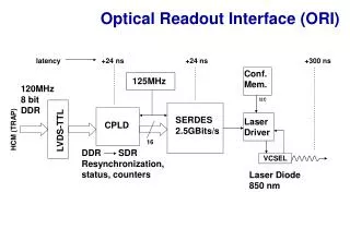
PLD 106 Mbps optical link receiver 7 program lines + 6 control lines NRZ signal Biphase Mark decoder and commands interpreter Incoming optical signal 53 MHz clock Multi chip module Signal processing PLL Outgoing optical signal Data Equalization logic (Only for testing) 1.06 Gbps optical link transmitter (daughter card) Data bus Data bus Figure 3: Sketch of the Optical Readout and Control Interface Board for the BTeV pixel detector.
PIN photodiode Mitel 1A354 Biphase Mark signal recovered (CMOS levels) 4 MAX999 The 106 Mbps optical link receiver is a very low noise circuit by itself, because the PIN photodiode is being used in photovoltaic mode, i. e. the PIN photodiode doesn't need to be biased, avoiding the dark current and the noise produced by the power supply used to do the biasing. The PIN photodiode delivers about 0.45mA/mW. The current flows through the 195 ohms resistor, then the discriminator receives a signal of about 114mV peak to peak, which is enough to make work the discriminator, which has a hysteresis of +/-5 mV around a threshold of 30mV. Figure 4: 106 Mbps optical link receiver. Comment: Iris Abt from Hera-B experiment told to Sergio Z. that their Pin photodiode has been affected by tracks crossing it. The 106 Mbps optical link needs at less 300 microamps (2*10**6e- per ns) to generated a one. So, we believe this receiver will be insensitive tracks crossing it. Tests will be carrying on to demonstrate it.
Non-Radiation Hard Version (TOP VIEW) Power connector Data [16..1] Outgoing optical signal Finisar Module FTM-8510 HP G-Link transmitter HDMP-1032 Serial signal Control Bus • Figure 5: Sketch of the Daughter board based on the HP G-link transmitter HDMP-1032. The continuos line represent parts on the top of the daughter card, while the dashed line represent the connectors on the bottom.
Radiation Hard Version (TOP VIEW) Power connector Data [16..1] Outgoing optical signal CHFET serializer developed by Peter Denes at CERN (Switzerland) Control Bus VCSEL CMOS to PECL translator Serial signal Diff. clock CMOS clock Figure 6: Sketch of the Daughter board based on the CHFET serializer and a HFE4080 Honeywell VCSEL. The continuos line represent parts on the top of the daughter card, while the dashed line represent the connectors on the bottom.
Performance of the first prototype of the optical readout and control interface • VCSEL Driver performance The VCSEL driver in the 106 Mbps optical link transmitter was designed to get a minimum variation of optical power between the Mitel VCSELs 1A444: -VCSELs driven with current produces 80% optical power variation. -VCSELs driven with voltage produces only 25%. (a) (b) Figure 8: Optical signals when we drive the Mitel VCSELs 1A444 with voltage. (a) Optical signal from VCSEL1 at 103 Mbps and (b) Optical signal from VCSEL2 at 103Mbps.
Performance of the 106 Mbps optical link transmitter and receiver (a) (b) (c) Figure 9: Optical signal carrying the inverted Biphase Mark code. (a) Eye pattern, (b) Jitter and (c) Rise and fall time of the optical signal transmitted. Also Fig. 9c is showing the NRZ signal sent. (a) (b) (c) Figure 10: Signal recovered carrying the inverted Biphase Mark code. (a) Eye pattern, (b) Jitter and (c) Rise and fall time of the 106 Mbps optical link receiver. Also Fig. 10c is showing the NRZ signal recovered.
Performance of the 1.06 Gbps optical link transmitter and receiver Figure 11: G-Link, Optical signal carrying the 16 data bits. (a) Eye pattern, (b) Jitter and (c) Rise and fall time of the 1.06 Gbps optical link transmitter. To test the 1.06 Gbps optical link it was generated an walking one pattern. In Fig. 12 is shown the pattern recovered by the 1.06Gbps receiver. Figure 12: Walking one pattern recovered.
Test Boards Figure 14: Optical Readout and Control Interface board. Figure 13: VCSEL driver. To test the 106 Mbps optical link with the MCM transmission was improved by making a board that has the protocol generator, BME and the VCSEL driver. Figure 15: Optical interface board. Figure 16: G-Link receiver.
Sending commands to program the MCM To test the readout and control interface, we use the PLD to improve transmission by making a board that has the protocol generator, BME and the VCSEL driver to be able to receive the commands from the Data Generator used to program the MCM. The PLD is translating each bit of the parallel frame in the Data Generator into a serial frame with 7 bits of protocol and later the serial frame is translated into BMC. 6 bits BCO lag (000010) , 4 bits CHIP ID (0100)and 1 bit Operation mode (0) Figure 17: Commands to program the BCO lag, CHIPID and Mode of operation. These commands are programmed in the Data Generator DG2020. 6 bits BCO lag (000010) , 4 bits CHIP ID (0100)and 1 bit Operation mode (0) Figure 18: Output commands (Logic analyzer) from the optical readout and control interface board. This board will be connected directly to the MCM.
Figure 19: Output commands (oscilloscope) from the optical readout and control interface board. This board will be connected directly to the MCM. Shiftin1 recovered ShiftClk recovered ShiftClk from DG2020 Figure 20: Radiation test result on the HFE4080 Honeywell VCSEL, courtesy of Peter Denes, CMS at CERN.
Tasks - Making work the multi-chip module with one FPIX1 on it to characterize it. - Connect the optical readout and control interface board with the MCM to characterize it. To see if the optical links produce some variation in the results. - Characterize with the optical readout and control interface the MCM with 5 FPIX1 chips on it.