Download
1 / 41
410 likes | 582 Vues
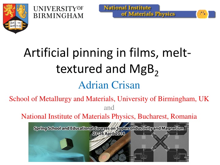
Artificial pinning in films, melt-textured and MgB 2. Adrian Crisan School of Metallurgy and Materials, University of Birmingham, UK a nd National Institute of Materials Physics, Bucharest, Romania. CONTENTS. Motivation YBCO (REBCO) films and coated conductors MgB 2 Melt-textured 123.

E N D
Artificial pinning in films, melt-textured and MgB2 Adrian Crisan School of Metallurgy and Materials, University of Birmingham, UK and National Institute of Materials Physics, Bucharest, Romania
CONTENTS • Motivation • YBCO (REBCO) films and coated conductors • MgB2 • Melt-textured 123
Motivation Energy efficient devices and equipment (magnets, motors, transformers, power lines) High Tc superconductors Low cost, High critical current Losses (dissipation): Movement of flux lines(Lorenz force, Thermal fluctuations) Solution: blocking flux lines (pinning) on various types of defects, natural and/or artificial Nanoengineered pinning centres
YBCO(REBCO) films and coated conductors YBCO films (Coated Conductors) have many types of natural pinning centres (i.e., they may occur naturally during growth process However, for many foreseen applications, especially in high magnetic fields, critical current still need improvement, hence larger FP, hence ARTIFICIAL PINNING CENTRES S.R. Foltyn et al, Nat Mater 6/9 (2007) 631.
Substrate decoration 5 4 3 2 1 1- substrate; 2- nanodots; 3- SC film; 4- columnar defects; 5- dislocations 2001 – A. C. and H. Ihara, Jap. Patent #3622147, EU and USA; A. C. et al. APL 79, 4547 (2001), APL 80, 3566 (2002), IEEE Trans. Appl. Supercond. 13, 3726 (2003); M. Ionescu,…, and A.C. J. Phys. D: Appl. Phys. 37, 1824 (2004)
Quasi-superlattices (quasi-multilayers) 2002 – A. C., seminar AIST (unpublished) 2004 – T. Haugan et al, (USAFRL), Nature, 430, 867 2005 – B. Holzapfel group (Dresden) J. Appl. Phys. 98, 123906.
Materials used up to now on Tl-based films, YBCO, ErBCO • substrate decoration: Ag– AIST Tsukuba (A. C.), Univ. Wollongong Australia (Ionescu, Dou, A. C.);MgO- AIST Japan (Badica and A. C.);Y2O3– CREST Japan (Matsumoto), Barcelona (Puig, Obradors), Dresda (Holzapfel);Ce2O3– AIST Tsukuba (Nie, Yamasaki);Ir– USA Univ. and Nat. Lab. consortium.; Au,Pd, LaNiO3– Univ. Birmingham (A. C.) • quasi-superlattices approach: Y2BaCuO5– USAFR, Wright-Patterson (Houghan);Y2O3– USAFR, Dresda; YSZ; BaTMO3(TM = transition metal = Ir, Ti, Zr, Hf);TM– Dresda; Au, Ag, Pd, LNO, PrBCO, ns-YBCO- Univ. Birmingham (A. C.) • impurity addition to targets: BaZrO3 – many groups (Cambridge & Los Alamos, ORNL, CREST-Japan, Univ. Birmingham & Univ. Turku Finland, etc..); BaNb2O6 ,BaSnO3– CREST Japan (Matsumoto); RE3TaO7(RE = rare earth = Er, Gd, Yb); - Univ. Cambridge & Los Alamos (J. McManus-Driscoll); double-perovskites YBa2NbO6(Cambridge)Gd2Ba4CuWOy– Univ. Birmingham & Cambridge (A. C.); combination of two-three types of impurities
Substrate decoration Distribution of the Ag nano particles deposited at 400o C by 15 laser pulses
Field dependence of critical current density at 77.3 K of pure YBCO film (open squares) and of the film grown on substrate decorated with 15 laser pulses substrate (full circles).
STO YBCO Columnar growth of YBCO on Ag Nanodots AFM-side view- of YBCO grown on (from left to right): Au nano—dots decorated substrate, Ag nano—dots decorated substrate and on bare substrate.
Y2O3 HRTEM showing the Cu-O planes and a large Y2O3 precipitate
Cross-sectional TEM image, showing c-axis correlated defects, arrow indicates c-axis. Mis-orientation in the boundary area
High-resolution cross-sectional TEM image of the substrate-film boundary. A nano-particle can be seen near the substrate High-resolution cross-sectional TEM image of the substrate-film boundary.
Columnar structure formed from the substrate Columnar structure
a) STEM image and element mapping of b) O2, c) Ba, d) Ag, e) Cu, f) Y
High-resolution TEM image of PBCO/YBCO multilayer near the film substrate interface, arrow and circle point to a PBCO nano-particle. A grain boundary along the c-axis.
Mis-orientated grain observed in the cross section TEM image. Defects in the middle of the film
BZO-doped YBCO and multilayer architectures of BZO-doped YBCO films High resolution of cross section TEM image of the film deposited at low temperature, BZO nano-particles are visible, and marked by circles. BZO nano-particles in the YBCO matrix of the film deposited at 780o C
Cu-O Cross section TEM image of BZO-doped YBCO film deposited at 800o C, clearly visible columnar structures (nano-rods) along the c-axis are formed Formation of Cu-O nano-particle found in the YBCO matrix of the film
EDX mapping of the BZO-doped YBCO film using STEM mode, a) STEM image, b) mapping of Ba, c) mapping of Cu, d) mapping of O, e) mapping of Y and f) mapping of Zr
Cross section TEM image of BZO-doped YBCO film near the substrate, arrow shows the c-axis of YBCO Formation of BZO nano-rods in the mildle area of the film, arrow shows c-axis
Short and long nano-rods grows together inside the YBCO matrix, along the c-axis. The BZO nano-rods started growing from the STO substrate, along the c-axis (arrow)
Some of the nano-rods are long, larger than the cross section of the image, arrow indicates c-axis Stacking fault found in high resolution TEM image
15Ag/BZO-doped YBCO multilayer architecture BZO nano-rods and nanoparticles in the YBCO matrix Cross section image of (15Ag/1 μm BZO-doped YBCO)x2, arrow shows c direction
Co-existence of Y2O3 (circle) and Cu rich phase (rectangular) and/or BZO phase. Defects caused by CuO2 and/or BZO phase observed in the middle area of the film.
A cross section TEM image near the STO substrate, arrow show the c-axis of YBCO A distorted area near the STO substrate, the c-axis is indicated by arrow
BZO nanoparticles and nano-rods BZO nano-rods entangled with columns of YBCO due to Ag-induced columnar growth
1.5 μm BZO doped YBCO / 30 nm STO/ 1.5 μm BZO doped YBCO on Ag decorated (15 pulses) STO substrates
Pinning in MgB2 • MgB2 wires are produced by various variants of Powder-In-Tube (PIT) process • Increase of Hc2 and Jc using nano—phase additions in the precursors in the initial stage • Carbon doping: amorphous, nano-diamond, carbon nanotubes • Ta, Ti, Zr impurity atoms used for absorbtion of H, to form e.g., ZrH2, preventing the formation of harmful MgH2 impurity
Addition of nano-Silicon • Best doping: SiC nanoparticles (up to 13-14 mol%) - B-rich phase - Mg2Si secondary phase - O- and Si- containing matrix • Silicon oil liquid precursor - Si formed Mg2Si - C substitutes B sites • Many other substitutions tried
Melt-textured REBa2Cu3O7 • Elemental 123: YBa2Cu3O7, NdBa2Cu3O7 • Mixed ternary light rare earth LRE–Ba2Cu3Oy (LRE = Nd, Eu, Sm, Gd) compounds (NEG-123, NSG-123, SEG-123) have twice irreversibility line (critical current density). • All these elements tend to sit on both the rare earth- and Ba-sites in the matrix and to form so called LRE/Ba solid solution. • Moreover, one can vary the LRE elemental ratio. Due to differences in the LRE ion sizes, the LRE ratio variation, especially in ternary composites can affect the local tensions in the matrix and contribute to the pinning performance. • Microstructure observations clarified that one can create nanoscale arrays in these materials and dramatically improve pinning at high magnetic fields
Besides, the melt-process technology enables introduction of non-superconducting secondary phase particles, RE2BaCuO5 “RE-211” that were found to enhance pinning at low magnetic fields. • ZrO2 ball milling of LRE-211 particles led to nanoscale 211 phase • Such particles (in the size of 70–150 nm) not only survived the melt-texturing process but also further reduced their size up to 20–50 nm. • Micro-chemical analysis identified these defects as Zr-rich ZrBaCuO and (NEG, Zr) BaCuO ones
The effect of Zr in the particles size diminution stacks obviously in the chemical inertia of Zr in the superconductor matrix • Creating nanoscale particles based on some other inert elements, like MgO or adding fine Y2Ba4CuZrOy particles to RE-123 confirmed validity of this hypothesis. • Use of the initial powder composed of the nano-sized REBa2CuZrOy particles and 35 mol% of sub-micron Gd-211 precipitates led to the super-current density around 270 kA/cm2 at 77 K.
nanoparticles from the same chemical group, namely Mo, and Nb: MoO3and Nb2O5 • Other family of nanoscale inclusions (RE)2Ba4CuMOy(where RE = Y, Sm, Gd, Nd, and M = Nb, Ta, W, Mo, Zr, Hf, Ag, Sb, Sn, Bi) were shown to improve drastically the properties of melt-textured 123