Download
1 / 4
130 likes | 737 Vues
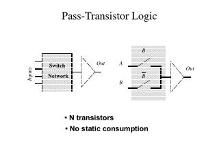
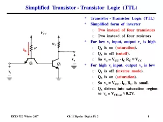
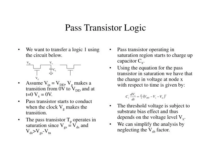
We want to transfer a logic 1 using the circuit below. Assume V in = V DD , V g makes a transition from 0V to V DD and at t=0 V x = 0V. Pass transistor starts to conduct when the clock V g makes the transition.

E N D
We want to transfer a logic 1 using the circuit below. Assume Vin = VDD, Vg makes a transition from 0V to VDD and at t=0 Vx = 0V. Pass transistor starts to conduct when the clock Vg makes the transition. The pass transistor Tp operates in saturation since Vgs = Vds and Vds>Vgs-Vtn Pass transistor operating in saturation region starts to charge up capacitor Cx. Using the equation for the pass transistor in saturation we have that the change in voltage at node x with respect to time is given by: The threshold voltage is subject to substrate bias effect and thus depends on the voltage level Vx. We can simplify the analysis by neglecting the Vsb factor. Pass Transistor Logic Vin Vx Cx Vg
Pass Transistor Logic • If we integrate the expression describing Cx we can solve for Vx.
The variation of the node voltage Vx as a function of time shows that if the voltage at node x cannot exceed a maximum of The above expression assumes that VSB is at logic 0. What would be the expression assuming a changing VSB since the source/drain voltage changes? The pass transistor turns off when Vx=Vmax since at this point the gate-to-source voltage is equal to the transistor’s threshold voltage. We need VGS>Vtn for ON. There are several possible states the terminals could be in: VG=0=Vin=Vx, VG=VDD with Vin =Vx=0, VG=VDD=Vin, with Vx=0 etc. Pass Transistor Logic VG Vx Vin
The nMOS device therefore passes good 0s and poor 1s since the source cannot be pulled to a value above VDD-Vtn (the threshold drop). When the source voltage rises VSB is not equal to zero any more an body effects occur. The threshold drop tends to violate noise margins. The pMOS device passes good 1s and poor 0s. Vx of the pMOS drops to below |Vtp| and the transistor cuts off. pMOS devices thus pull down to only |Vtp| above ground (GND). Why isn’t, Vmax4 VDD-Vtn1-Vtn2-Vtn3-Vtn4? What would happen if we configured the series devices above to have each drain/source drive the next device’s gate? Pass Transistor Logic VDD Vmax3=VDD-Vtn4 VDD V1 V2 V3