Download
1 / 22
220 likes | 424 Vues
PV Panels and P N Junctions. How PV Panels work Or An Introduction to the World of Microelctronics. What are PV Panels?. PV Panels are thin layers of Silicon that have been designed to convert solar energy into electricity. Silicon is a semi conductor.

E N D
PV Panels and P N Junctions How PV Panels work Or An Introduction to the World of Microelctronics
What are PV Panels? • PV Panels are thin layers of Silicon that have been designed to convert solar energy into electricity. • Silicon is a semi conductor. • Semi conductors are elements that under certain conditions conduct electricity and under others do not.
Second most abundant element on Earth. Elemental silicon transmits more than 95% of all wavelengths of infrared light The essentials Name: silicon Symbol: Si Atomic number: 14 Atomic weight: 28.0855 (3) Group number: 14 Period number: 3 Silicon basics
Complete Valence Bands • All elements want to have their outermost band complete, or no missing electrons. • For all elements with the exception of Hydrogen and Helium that outermost band will require 8 electrons. • Due to the Heisenberg Uncertainty Principle the atoms are able to share electrons in their outermost shells.
Crystal Lattices • Silicon is solid at room temperature and its atoms are arranged in a lattice type of structure. • Since Silicon has 4 electrons in its outer band it is looking to share or borrow 4 electrons from another atom or atoms so that it has its complete outer band of 8 electrons.
Can That Really Happen? • This will happen but only under specific conditions (Si is a semi conductor). • This EHP (electron hole pair) can be caused by light or heat to name a few. • In Si the bad gap is 1.12 eV. • At room temperature there will be 145 trillion EHPs at any one time.
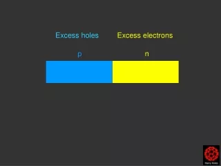
Types of Doping • Impurities are added on purpose to increase electron mobility or flow. • B, In are Group III dopants. (green) • These elements have only 3 electrons in their outer band so a hole is created. P-type Si. • P, As, Sb are Group V dopants. (blue) • These elements have 5 electrons in their outer shells so a electron is free to move. N-type Si.
Types of Electrical Flow • Current is the measure of the flow of electrons. • There are two ways that electricity can flow. • Conduction band electron current • Valence band hole current.
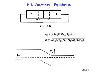
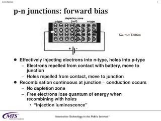
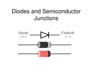
PN Junctions • When P-type Si is placed next to N-type Si you have what is called a PN junction. • PN junctions are at the heart of things like PV panels and electrical diodes. • The band gaps in N-type and P-type Si are different however due to the presence of different dopants.
Band Gaps • Different dopants mean that there are different band gaps. Boron Doped Phosphorus Doped
PN Junctions • When the two Si types are placed next to one another a depletion region is formed. • The depletion region is created when the free electrons from the N-type side rush over to fill the holes left in the P-type side. • The depletion regions have no free carriers and therefore resist electron flow.
Depletion Regions • If the size of the depletion region is “large” enough then the electrons will not be able to cross the gap. • Think of it like the Grand Canyon vs. rain water rushing towards the storm drain. • No one* would consider jumping the Grand Canyon, but a rain water stream most can handle. • The same is true of electrons.
Biasing the Junctions • If the junction is biased (a voltage is applied to either side) then current will flow. This is where the photons come in to play in the PV panels. • Applying the voltage changes the electric Grand Canyon into that small storm water stream.
By applying a positive voltage to the P-type side and a negative voltage to the N-type side the depletion region shrinks dramatically. This is because more free carriers are added to the system. Biased PN Junctions
Sunlight and PV panels • The photons that are raining down on us from the sun are little packets of energy. • There are some packets which just happen to be at exactly 1.12 eV. • The photons from the sun can therefore be harnessed to increase the number of free carriers in the Si. • More free carriers means the junction is biased and current can flow across the gap.