Download
1 / 21
210 likes | 231 Vues
Mobile charge carriers Density of states Law of mass action Intrinsic Fermi level Intrinsic carrier concentration Doping of semiconductors. Lecture 3: Electrons in semiconductors II. In intrinsic semiconductors the electron density is equal to the hole density ( n i and p i ).

E N D
Mobile charge carriers Density of states Law of mass action Intrinsic Fermi level Intrinsic carrier concentration Doping of semiconductors Lecture 3: Electrons in semiconductors II Semiconductor Applications L3
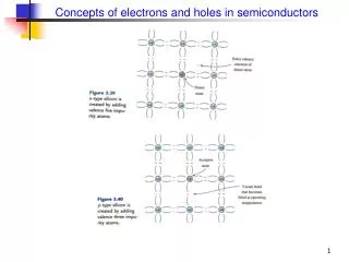
In intrinsic semiconductors the electron density is equal to the hole density (ni and pi). An intrinsic semiconductor is one that contains a relatively small amount of impurities compared with thermally generated electrons and holes. An extrinsic semiconductor, conversely, is a material which contains large amounts of impurities. Intrinsic and Extrinsic Semiconductors Semiconductor Applications L3
Mobile carrier density= n + p Mobile charge carriers Electrons in the conduction band (density, n) carry current Semiconductor Applications L3 Holes in the valence band (density,p) carry current
Hole DOS Electron DOS Hole concentration Electron concentration Density of states and Fermi function Semiconductor Applications L3
The intrinsic carrier concentration refers to the electrons (holes) present in the conduction (valence) band of a pure semiconductor. It is dependent on the magnitude of the bandgap and the temperature as well as the effective masses. The concentration of electrons in the conduction band is: Ne(E) is the electron density near the conduction band edge, f(E) is the Fermi function Mobile charge carriers Semiconductor Applications L3
The concentration of electrons in the conduction band can hence be written: Mobile charge carriers Semiconductor Applications L3 Effective density of states at the conduction bandedge
The carrier concentration is known when EFis calculated. To find the intrinsic carrier concentration required finding the hole concentration p as well. Then hole distribution function is: Then: Mobile charge carriers Semiconductor Applications L3
In intrinsic semiconductors the electron concentration is equal to the hole concentration, an electron in the conduction band leaves a hole in the valence band. The product np is independent of the position of the Fermi level and is dependent only on the temperature and intrinsic properties of the semiconductor. This is known as the Law of mass action If n increases, p must decrease. np=ni2 For the intrinsic case n=ni=p=pi, we take the square root of the above equation: The law of mass action Semiconductor Applications L3
Setting n=p we can obtain the Fermi level position. The intrinsic Fermi level denoted by Efi The Fermi level of an intrinsic material lies close to the midgap. In calculating mh* and me* the number of valleys and the sum of heavy and light hole states have to be included. Intrinsic Fermi level Semiconductor Applications L3
The carrier concentration increases exponentially as the bandgap decreases. Notice the strong dependence on temperature. In electronic devices where current has to be modulated, the concentration of intrinsic carriers is fixed by the temperature and this therefore detrimental to device performance. Carrier concentration: Remarks Semiconductor Applications L3
Once the intrinsic carrier concentration increases to ~1015cm-3, the material becomes unsuitable for electronic devices due to the high leakage current arising from the intrinsic carriers. High bandgap semiconductors such as diamond (C), and SiC have attracted growing interest. They can be used in high temperature applications. Pure semiconductors have a low concentration of mobile carriers: Typically ~1011cm-3 for intrinsic semiconductors And ~1021cm-3 for metals. The addition of impurities – doping – can be used to change the conductivity of semiconductors. Intrinsic carrier concentration Semiconductor Applications L3
Calculate the position of the intrinsic Fermi level in Si at 300K. The density of states effective mass of the combined six valleys of silicon is: The density of states mass for the valence band is 0.55m0. Hence the intrinsic Fermi level is given by: The Fermi level is then 13.2meV below the centre of the mid-bandgap. Example: Intrinsic carriers Semiconductor Applications L3
There are two kinds of dopants: Donors, which donate an electron to the conduction band. (n-type) Acceptors, which accept an electron from the valence band – and therefore create a hole. (p-type) A donor atom should have one or more electrons in its outer shell than the atom it replaces. In silicon (a four valent atom) the addition of a pentavalent atom means the remaining fifth electron now sees a positively charged ion to which it is attracted. The attractive potential is simply: Doping of semiconductors Semiconductor Applications L3
The lowest-energy solution for this problem is the ionisation energy: Notice the effective mass m* is used. The energy level is measured from the bandedge. Donor impurities Semiconductor Applications L3
The simple hydrogen model cannot account for the details of ionisation energy, particularly for the deep impurity levels in semiconductors (ionisation energies >3kT). Calculated values do predict the correct order of magnitude of the true ionisation energies for shallow impurity levels. For shallow impurities in Si and GaAs, there is usually enough thermal energy Ed to ionise all donor impurities, and thus provide an equal number of electrons in the conduction band. This condition is called complete ionisation. Under complete ionisation the electron density (n) equals the donor concentration (ND). Carrier freezeout occurs if donor (acceptor) electrons (holes) are tied to there respective lattice sites. Limitations of hydrogen formalism Semiconductor Applications L3
Another effective mass ms*, the conductivity effective mass is introduced to describe how electrons respond to external potentials. This mass is used for donor energies as well as for charge transport in an electric field. For direct bandgap semiconductors, this is the effective mass. For indirect materials such as silicon the conductivity mass is: Reminder: The density of states mass represents the properties of the electrons at a constant-energy surface in the band structure. Donor impurities Semiconductor Applications L3
The acceptor levels are produces when impurities that have a similar core potential as the atoms in the host lattice, but have one less electron in the outer shell, are introduced. Group III elements can act as acceptors in Si or Ge. Under complete ionisation the hole density (p) equals the acceptor concentration (NA). Acceptor impurities Semiconductor Applications L3
Summary of donors and acceptors Semiconductor Applications L3 Doped semiconductors are referred to as extrinsic semiconductors.
We can now write the Fermi level in terms of the effective density of states NC and the donor concentration Nd: Recall: Therefore: Similarly for shallow acceptors p=NA and: For higher donor concentration, the smaller the energy difference (EF-EC), the Fermi level moves closer to the bottom of the conduction band. Extrinsic Fermi Level Semiconductor Applications L3
Considering material that have a dominance of donors (n-type) or acceptors (p-type). There is no longer equality between the electrons and holes: The law of mass action still holds – and only changes at high doping levels: As indicated, when the semiconductor is doped n-type (p-type), the Fermi level moves towards the conduction (valence) bandedge. When the Fermi level approaches the bandedge, the Boltzmann approximation is not very good and the simple expressions relating the carrier concentration and Fermi level are not very accurate. Extrinsic Carrier Density Semiconductor Applications L3
Mobile charge carriers Density of states Law of mass action Intrinsic Fermi level Intrinsic carrier concentration Doping of semiconductors Summary of lecture 3 Semiconductor Applications L3