Download
1 / 36
360 likes | 564 Vues
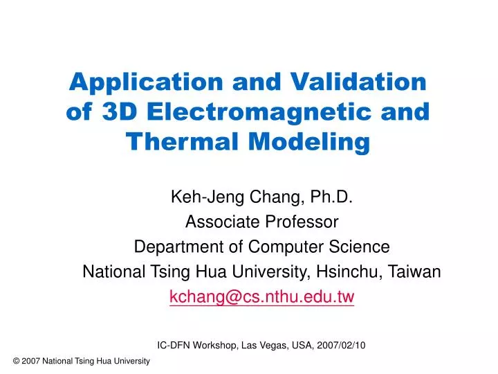
Keh-Jeng Chang, Ph.D. Associate Professor Department of Computer Science National Tsing Hua University, Hsinchu, Taiwan kchang@cs.nthu.edu.tw. Application and Validation of 3D Electromagnetic and Thermal Modeling. Acknowledgements.

E N D
Keh-Jeng Chang, Ph.D. Associate Professor Department of Computer Science National Tsing Hua University, Hsinchu, Taiwan kchang@cs.nthu.edu.tw Application and Validation of 3D Electromagnetic and Thermal Modeling
Acknowledgements The authors want to thank the following institutes for providing this research with generous resources: • National Science Council, Taipei • Ministry of Economic Affairs, Executive Yuan, Taipei • Ministry of Education, Executive Yuan, Taipei • TSMC, Hsinchu • UMC, Hsinchu • Silvaco International, Santa Clara • Clear Shape Technologies, Sunnyvale
Major References • Silvaco International, “TCAD for Flat Panel Display,” Technical Presentation Slides, Jan. 2006, Hsinchu, Taiwan. • Y.H. Tai, Design and Operation of TFT-LCD Panels, ISBN 957-11-4291-3 (Chinese Language), June 2006, Taipei, Taiwan. • K.J. Chang, “Accurate On-Chip Variation Modeling to Achieve Design for Manufacturability,” 4th IWSOC, July 2004, Banff, Canada. • K.J. Chang et al., “Verifying On-Chip Inductance Extraction with Silicon Measurement,” www.eetimes.com, Nov. 2003. • J.F. Huang et al., “Modeling Sub-90nm On-Chip variation Using Monte Carlo Method for DFM,” 12th ASP-DAC, Jan. 2007, Yokohama, Japan. • J. Xiong et al., “Robust Extraction of Spatial Correlation,” 6th ISPD, April 2006, San Jose, USA. • K.M. Cham et al., Computer-Aided Design and VLSI Device Development, 2nd edition,Kluwer ISBN 0-89838-277-7, 1988.
Outlines • The emerging needs of 3D models • 3D research summary • Applications of 3D models • Validations of 3D models • In a nutshell
The Emerging Needs of 3D Models • A “fishbone” viewpoint of 3D research subjects Optical/optoelectrical Biological/medical Mechanical DC+TEM (deterministic) CFD/naval 3D Statistical Art/social Thermal Full-wave (deterministic) Molecular/atomic Material/chemical
3D Research Summary (Algorithms) • Modeling (1D, 2D, 3D) • Empirical • Simulated • Simulations • Finite difference (with or without time domain) • Finite element • Boundary element • Monte Carlo / Markov / Brownian • Governing mathematics • Maxwell’s • Poisson / Laplace • Fourier • Band gap • et al.
3D Research Summary (Inputs/Outputs) • Models based on profiles/structures of nanodevices • Dimensions on x-axis, y-axis, and z-axis • Cartesian coordinates dominate 3D modeling in electronics • Material properties • Permittivity • Permeability • Stress • Resistivity • Leakage • Thermal conductivity • et al. • 3D mechanical / thermal / electromagnetic nanodevice models • Electrical and non-structural model/characterization • SPICE-level circuit simulations
3D Research Summary (Bright Future) • Commercially successful (profitable) and sustainable stories in 3D modeling for the electronics • Ansoft • Ansys • Silvaco • Matlab • Sigrity • Brion (merged to ASML) • Numerical Technologies (merged to Synopsys) • Etc.
Applying 3D Models to TFT-LCD Vertical structure of a pixel and its equivalent circuit
TFT-LCD Designs to Prevent Mura Note: Validating mura product defects through 3D TFT-LCD models is an on-going research in NTHU-CS. Source: Silvaco ‘06
Manufacturable Through Silicon Vias The growing popularity of trough silicon vias (TSV) and on-chip spiral inductaors. Source: P. Franzon, NCSU, ‘05
1D Thermal Modeling Performed in NTHU-CS ‘06
3D Thermal Modeling (1/2) • Heat sink (30oC) on top of the silicon chip while the CMOS pn junction is at 77oC.
Deterministic Eectrical 3-D Modeling DRC-clean nanometer circuit layouts Current pseudo 3D layout parameter extraction (LPE) New 3D layout parameter extraction (LPE) SPICE decks SPICE decks Timing simulations and clock speed comparisons (We suggest that the new 3D LPE should be adopted if the compared difference is > 10%.)
3D Capacitances by 3-D Tools Figure 1. Complex nanometer 3D profiles for parasitic capacitance models.
Nanometer Ring Oscillator • Ring oscillator layout (left) uses Prof. His-Pin Ma’s design • The corresponding schematic (right)
Current EDA vs. 3D EDA Differences • The above circuit performance degradation data are real if the 3D models are accurate. • The pseudo-3D EDA tools are implied to be too optimistic and should be replaced with the new 3D EDA tools. • The 3D EDA tools (not yet validated) are more pessimistic and therefore are likely to be more realistic.
Applying and Validating 3D Models (1/4) Source: UMC ‘03
Physical Views of Sub-100nm VLSI • 2-D and 3-D views of sub-100nm physical structures (Courtesy: UMC, 2006)
Varying Nanometer BEOL Profiles Source: IWSOC ‘04
Material Properties as Profiles Source: IEDM ‘06
Validating or Failure in Validating? Source: ASP-DAC ‘07
Gate Oxide On-Chip Variations Source: IBM/UCLA ISPD’06 paper
Lithographic Imaging in Sub-100nm • Courtesy Porf. KY Tsai of NTUEE, 2006
Resolution Enhancement Tech (RET) • RET includes Optical Proximity Correction (OPC)
3-D Modeling and Predicting RET • Profiles through Resolution Enhancement Technology and Detailed Fourier Transform (not yet validated)
In a Nutshell • 3-D electrical modeling for resistance, capacitance, thermal, inductance, and transmission lines of TFT-LCD and sub-90nm devices are performed but more are planned. • 3-D lithographic modeling for sub-100nm with National Taiwan University and commercial companies is started. • 3-D modeling of etching/CMP or reliability not started yet.