Download
1 / 16
200 likes | 409 Vues
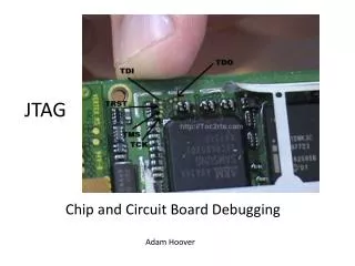
JTAG. Chip and Circuit Board Debugging. Adam Hoover. Background. 1980’s explosion of embedded computing products. Background. Mass production of chips … how to test in bulk?. Mass production of products … how to test in bulk?. Background.

E N D
JTAG Chip and Circuit Board Debugging Adam Hoover
Background 1980’s explosion of embedded computing products
Background Mass production of chips … how to test in bulk? Mass production of products … how to test in bulk?
Background Chip fails in a product … how to find which part failed?
Background During product development … how to debug/observe code?
How to see inside a chip? X-ray Can see traces, detect breaks How to test functionality? Used for inspection Non-break failures?
How to see inside a chip? Oscilloscope Pins getting smaller and smaller Lots of pins! Pins underneath the chips How to affect, record?
Boundary Scanning Dedicate some pins to test and debug Read voltages from other pins or circuitry inside chip via debug pins When turned on, in debug mode; when turned off, operate normally
Background Industry manufacturers were all making custom solutions JTAG = Joint Test Action Group IEEE 1149.1 Standard Test Access Port (TAP) and Boundary-Scan Architecture (mouthful, let’s just call it JTAG)
JTAG pins Input/output voltages Shiftedthrough latches on pins around the boundary of the chip TDI = input TDO = output TCK = clock TMS = test mode select (turn JTAG on/off)
Multiple chips Connect chips in series
Details Some default instructions: BYPASS (TDO = TDI) SAMPLE/PRELOAD IDCODE(chip ID) INTEST (run internally hold pins) CLAMP/HIGHZ (voltage test) RUNBIST (built-in self test) … Shift in/out 1 bit at a time Buffer bits to form JTAG instruction (slow!) Execute JTAG instruction Dual-use some pins for more debugging options
On a product through-holes header
Software interface High-level IDE for processor programming and debugging Low-level (non-processor chips) Custom, anything in-between