Download
1 / 14
180 likes | 491 Vues
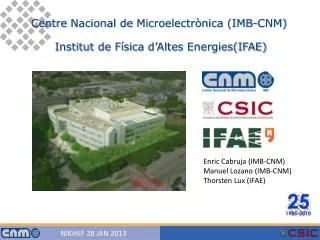
IMB-CNM (CSIC). Manuel Lozano CNM (CSIC) Barcelona, Spain. Centro Nacional de Microelectrónica Is a Public Research Organism that belongs to the Spanish Council for Scientific Research (CSIC) Located in Bellaterra, close to Barcelona (Spain) Devoted to Nano and Microelectronics

E N D
IMB-CNM (CSIC) Manuel Lozano CNM (CSIC) Barcelona, Spain
Centro Nacional de Microelectrónica Is a Public Research Organism that belongs to the Spanish Council for Scientific Research (CSIC) Located in Bellaterra, close to Barcelona (Spain) Devoted to Nano and Microelectronics Micro Nano Fabrication Facility (Clean Room) Departments: Micro and Nano Systems Silicon sensors and actuators Nanotechnologies Systems Integration Power devices Circuits and systems design Biomedical applications IMB-CNM Presentation
Clean Room 1.500 m2, class 100 to 10.000 Micro and nano fabrication technologies Three areas: Pure (CMOS) Noble metals allowed Nanoelectronics Processes 4'' complete 6'' partial (no full thermal processes) Available technologies: CMOS, BiCMOS, MCM-D, MEMS/NEMS, power devices Bump bonding packaging Silicon micromachining Packaging 200 m2, class 100 Laboratories Characterization and test DC and RF (up to 8 GHz) Wafer testing Thermography Radiation testing Reverse Engineering Simulation CAD Mechanical Workshop Chemical sensors Bio-sensors Radiation sensors Optical sensors IMB-CNM facilities
Thermal processes and CVD Ion Implantation PVD and Metallisation Lithography (proximity and stepper) Nano-lithography (electron beam, AFM and nano-imprint) Direct laser writing Dry etching Wet and dry micromachining Wet etching and cleaning In line test Wafer grinding and CMP Clean Room Equipment (more than 150 units) See full list at: http://www.imb-cnm.csic.es/
Wet and dry oxidations. Ion implantation B, P, As, N and Ar. Diffusion CVD Si3N4, polysilicon, SiO2, BPSG Metallization Al/Si, Al/Cu, Al/Cu/Si, TaSi, Ti, Ni, Au, Pt, Cr, Ag, a-Si, and Ge. Wet and dry etching Surface and bulk silicon micro mechanization Anodic bonding Packaging die bonding, wire bonding, SMD In line test Ellipsometry, interferometry, profilometry, four-point probes Photolithography contact/proximity, step and repeat, double side Nanotechnology AFM Electron beam Nano-imprint FIB (Focused Ion Beam) Clean room main processes
Simulators Sentaurus (Synopsys) Technology simulation Electrical simulation (Static and dinamic, Charge collection in 3D) Particle interaction: GEANT4, MCNP-X Technologies: P-on-N, N-on-P, N-on-N Pad, strip and pixels detectors High resistivity poly, capacitive coupling, two metal layers, two side processing Limited to 4 inches wafers Radiation hard devices: Oxygenated FZ and magnetic Czochralski silicon. Detector design, simulation, fabrication and characterization
Pitch adaptor production 10,000 pieces for ATLAS Inner Detector Endcaps in three years The biggest commercial contract of IMB-CNM/D+T WE contracted new technicians working only for this production Good experience ATLAS pitch adaptors
Double Side Detectors • Material • Silicon doping: n-type • Thickness: 800 microns • Resistivity: between 20 and 30 kW·cm • Electrode structures • Electrodes formed to run orthogonally on both sides of the silicon. • Electrode strip length: ~ 4 cm • Electrode strip pitch: 500 µm • Electrode strip width: 400 µm • Signal coupling: DC • Performance • Leakage current < 12 nA/cm2 at 20°C • Gettering process to reduce leakage current
3D pixel detectors for IBL • 3D pixel detectors for Insertable B-layer for ATLAS • Double side configuration • October 2009 common layout (compatible) • February 2011 end pre-series fabrication • March 2011 started pre-production for IBL • 2012 fabrication -> 8 months • Manufacturers: FBK (Trento) and CNM
1) Process backside of thick detector wafer (structured) implant. 2) Bond detector wafer on handle wafer. 3) Thin detector wafer to desired thickness (grinding & etching). 4) Process front side of the detector wafer in a standard (single sided) process line. 5) Etch handle wafer. If necessary: add Al-contacts. Leave frame for stiffening and handling, if wanted Ultra-thin detectors using SOI wafers
Participation in AIDA project • Procurement of strip detectors for the development of the telescope • With our (limited) budget we can provide a reasonable number of standard detectors (in 4'' wafers) for a telescope • And also test standard detector technology with advanced features (not all at the same time) • Thin devices (230 um) • Integrated fanins • IR "transparent" detectors (for laser alignment) • Resistive coupling capacitors (2D sensing)
Integrated fanins • 2 metals • Suitable dielectric under study
L1a L2a L3a L4a L5a L6a Y X P1 P2 P3 P4 P5 P6 1 L1b L2b L3b L4b L5b L6b Resistive material Resistive coupling detectors Al • Coupling capacitor made of poly • Readout at both sides • 2D sensitivity
IR transparent detectors • All layers optimized to increase IR laser transmission • Target 70% • Alignment of several layers using laser signal