Download
1 / 13
130 likes | 133 Vues
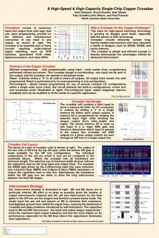
This paper outlines the design and simulation of a high-speed and high-capacity single-chip copper crossbar circuit. The advantages of copper interconnect technology are discussed, along with the electrical and physical characterization of the circuit. The paper also highlights the electrical results and failure analysis, which led to the discovery of missing diffusion patterns. Overall, the copper crossbar circuit achieved higher data rates, reduced latency, and smaller cell size compared to equivalent aluminum circuits.

E N D
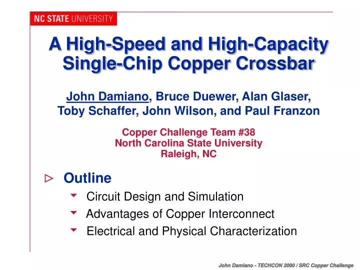
A High-Speed and High-Capacity Single-Chip Copper Crossbar • Outline • Circuit Design and Simulation • Advantages of Copper Interconnect • Electrical and Physical Characterization John Damiano, Bruce Duewer, Alan Glaser, Toby Schaffer, John Wilson, and Paul Franzon Copper Challenge Team #38 North Carolina State University Raleigh, NC
The Copper Crossbar • Function • Crosspoint switch with programmable, non-blocking connections between sets of input and output lines • Why a crossbar? • The inherently long interconnects can best demonstrate the benefits of advanced interconnect technology
Cell Design • Programmed through input lines • I/O connection set by writing “1” to latch • Latch outputs along output column combined OR-tree Cell Schematic Cell Layout • Reset & Pre-Configures provide fast erase & write Cell size (W x L) = 5.68 mm x 19.50 mm (two cells shown at right)
Interconnect Strategies • Input lines on M5, Output OR-tree on M3 • M4/M6 used as GND planes Global Strategy:Maintain R and Decrease Linewidth to Reduce C Capacitance Values for Crossbar Interconnect • Reduced RC load drops => Higher Performance • Reliability of Cu not an issue
Simulation Output for 2.0GHz square wave input Metric #1 - Data Rate maximum input signal frequency for the crossbar Reduced RC load using Copper interconnect enables higher data rate vs. Aluminum Copper: 5.3 Gb/s Aluminum: 4.0 Gb/s Aluminum Copper
Simulation Output for 2.0GHz square wave input Metric #2 - Latency Delay of signal from crossbar input to output Faster edge rate with Copper interconnect enables lower latency vs. Aluminum Copper: 370 ps Aluminum: 425 ps Aluminum Copper
Advantages of Copper Interconnect • Performance • Copper Interconnect enables 30% higher Data Rate and 15% lower Latency vs. Aluminum • Cell Size • Tighter metal pitch with same resistivity available with Copper Interconnect • Aluminum cell with equivalent performance would be 64% larger due to wider lines, increased pitch, and/or larger drivers • Significant for arrayed / SOC applications
Electrical Results • Input NOT passed to Output for all I/O configurations Input Output • VDD/VSS Diode characteristics NOT observed VDD-VDD & VSS -VSS VDD -VSS
Failure Analysis • Die stripped to substrate using HF to investigate VDD-VSS opens • Diffusion pattern, created by P20 reticle, discovered to be absent! • Only Diffusion pattern visible on die consists of Fill Shapes around original diffusion data Detail of pad cell How could this happen? Detail of crossbar array
Generating Fill Shapes A B’ B (A-B’)+B A-B’
Silicon vs. Layout Data pad cell layout pad cell silicon array layout array silicon
Failure Analysis • Crossbar pad cells compared to NCSU Team #16 - the diffusion pattern was dropped only for our die • Explains unusual electrical data - no active devices present • Only solution - new P20 (diffusion) reticle must be generated • Good News! UMC has agreed to re-order P20 reticle and start new Copper Challenge lot Team #38 pad cell Team #16 pad cell
Conclusions • Copper Crossbar circuit developed to exploit the advantages of copper interconnect technology • Crossbar design using copper interconnect achieved a higher data rate and reduced latency, with a smaller cell size vs. equivalent aluminum circuit • Puzzling Electrical Results from fabricated chips led to discovery of missing diffusion pattern • UMC re-run of Copper Challenge designs promises to yield functional die with advanced interconnect & high performance