Download
1 / 21
210 likes | 318 Vues
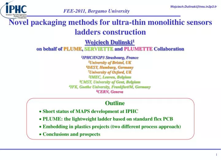
Novel packaging methods for ultra-thin monolithic sensors ladders construction. Wojciech Dulinski 1 on behalf of PLUME , SERVIETTE and PLUMETTE Collaboration 1 IPHC/IN2P3 Strasbourg, France 5 University of Bristol, UK 6 DESY, Hamburg, Germany 7 University of Oxford, UK

E N D
Novel packaging methods for ultra-thin monolithic sensors ladders construction Wojciech Dulinski1 on behalf of PLUME, SERVIETTE and PLUMETTE Collaboration 1IPHC/IN2P3 Strasbourg, France 5University of Bristol, UK 6DESY, Hamburg, Germany 7University of Oxford, UK 2IMEC, Leuven, Belgium 3CMST, University of Gent, Belgium 4IFK, Goethe University, Frankfurt/M, Germany 8CERN, Geneva • Outline • Short status of MAPS development at IPHC • PLUME: the lightweight ladder based on standard flex PCB • Embedding in plastics projects (two different process approach) • Conclusions and prospects
R.T. Monolithic Active Pixel Sensor: effective use of a thin epitaxial layer (10 – 20 µm) for MIP tracking past present Industrial availability of high resistivity substrate (epi) in a standard CMOS process Fast and more efficient charge collection should be radiation tolerant
Present status of MAPS: just one example of mature design • Binary sparsified readout sensor for EUDET beam telescope: > 2 cm2 active area, 0.7 Mpixel tracker • Medium speed readout (100 µm integration 10 kFrame/s) • Spatial resolution < 4 µm for a pitch of 18.4 µm • Efficiency for MIP > 99.5 % • Fake hit rate < 10-6 • Radiation hardness > 1013 n/cm2 (high resistivity epi substrate) • Easy to use, “off-shell” product: used already in several application • Recent newcomer : Ultimate sensor for STAR Microvertex upgrade (~4 cm2) • Radiation hardness: >1014 n/cm2 attainable? Mimosa 26
One of the main feature of MAPS Can be very thin (~25 µm of silicon in total) and still fully efficient! Problem: how to handle, interconnect and at the end built a low mass ladder with such a thin device?
PLUME concept: double-sided ladder (ILC compatible) • 2x6 Mimosa26 sensors • Standard flex PCB: kapton + Cu (two layers) • SiC foam for spacer between layers
PLUME thermal study: M26 parameters • “Rolling shutter”, column parallel processing: only processed pixel row dissipate power! • Total 730 mW (1/3 for pixel, discri and digital) • 250 mW/cm2(160 mW/cm2 for STAR Ultimate) • 1.1 µW/pixel (5-10 µW/pixel for time continuous shaping ~1 µs) • Power dissipation distributed unevenly: hot spots!
PLUME thermal study: simulations Hot spots with temperature of above 100 °C!
Effects of temperature distribution on electrical parameters: S-curve of Mimosa 26 on PLUME ladder
Add heat-spread layer? The best would be based on CVD diamond! Or carbon fibers, excellent also for mechanics…
SERVIETTE: use of UTCP by IMEC… • Stands for : • ULTRA THIN FILM CHIP PACKAGING • In short : • Off-the-shelf die • Thinned down to ± 20-30 µm • Packaged between two polyimide foils • Metallisation : fan-out • Circuit contact through vias Polyimide 2 • Result : • Flexible package • Thin : 50-70 mm • Embeddable in commercial flexible PCB Polyimide 1 - Partner restricted PTW Oct. 2010 - HUMAN++
UTCP flow: overview • Polyimide on rigid carrier with release layer (KCl) • Dispense/spin of BCB • Chip thinning • Placement (face up) of IC 60 mm • Photo definable polyimide spinning (20µm)) • Opening vias using lithography • Cleaning of contact pads • Metallization: TiW (50nm) + Cu(1µm) • Electroplating : Cu (5µm) • Lithography to pattern metal • Encapsulation polyimide spinning • Release from carrier
First results: Mimosa18 mechanical grade sample Submitted for fabrication more thana year ago, very slow progress since…
PLUMETTE: “standard” PCB process for chip embedding in plastic foils (R. de Oliveira, CERN) • Gluing between two kapton foils • Opening vias using lithography • Single module: intermediate tests • Metallization: Al (5-10 µm) • Lithography to pattern metal • Complete ladder assembling, laser cut along sensor edges • Gluing of another kapton foil for deposition of second metal layer 16
PLUMETTE: details of 1st, “redistribution” metal layer If too difficult for PCB-standard lithography (too small feature size), this post-processing step can be provided by CMOS foundry (discussion with AMS, 5th metal in 0.35 µm process)
PLUMETTE: details of 4 metal layer flex Impedance of readout lines (last metal, 100 µm width, 100 µm gap) as a function of kapton thickness: 100 Ωfor 60 µm thick kapton (last layer)
Future techniques: stitching (“one die per wafer”) Maximum length of monolithic ladder (8’ wafer): 10 –15 cm
Bonding pads On going work and future plans: use of Vertical Integration Process (3D Electronics) Sensor comprised of several active silicon layers: sensor, analog processing, digital processing, memory, optoelectronics layer… Total thickness of this stack is still ~50 µm! 20 µm 3-tiers, heterogeneous CMOS, ultra-thin and edgeless MAPS - Possible decrease of power per pixel (by order of magnitude): see Yavuz Degerli talk from FEE-2009 - Elimination of some “hot spots”
Conclusions • Ultra thin packaging technology seems to be interesting option for ultra light sensor ladders construction • It is the must, if one wants to take full profit from MAPS tracking performances (front-end mechanics is as important as front-end electronics) Outlook • Double-sided PLUME ladder by autumn 2011, followed by beam tests • Delivery of working Mimosa18 sensors embedded at IMEC: June/July ? • Delivery of single Mimosa26 embedded at CERN in June, full PLUME compatible ladder (six M26) in September/October • Stitching exercise next year?