Download
1 / 23
240 likes | 504 Vues
9 . Design of Multiple-input Op. Amp. Circuits. 9.1 Operational Amplifiers 9.2 Basic Operational Amplifier Circuits 9.3 Input resistance of Op. Amp. Amplifiers 9.4 Multiple-Input Operational Amplifier Circuit 9.5 Design of Multiple-Input Amplifiers . -.

E N D
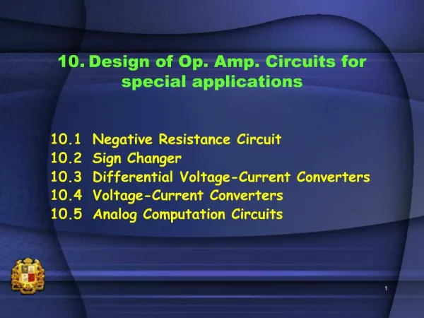
9. Design of Multiple-input Op. Amp. Circuits 9.1 Operational Amplifiers 9.2 Basic Operational Amplifier Circuits 9.3 Input resistance of Op. Amp. Amplifiers 9.4 Multiple-Input Operational Amplifier Circuit 9.5 Design of Multiple-Input Amplifiers
- Push-pull Emitter follower at the output + Op. Amp. input Impedance Very high ii = 0 R0= 0 v+ = v- Collector Constant current source ii = 0 Differential Amplifier Emitter Constant current source Amplifier voltage gain very high Output Impedance very low +Vcc 9.1 Operational Amplifiers Inverting Input (-) +Vcc output Non-InvInput (+) Inverting Input (-) Non Inverting Input (+) output -Vcc -Vcc • Therefore Operational Amplifier has • very high input impedance, Ri= a(or) ii = 0 • (2) very high voltage gain Av = 105 (or) v+ = v- • (3) very low output impedance R0 = 0
1. INVERTING AMPLIFIER 9.2 Basic Operational Amplifier Circuits 2. NON-INVERTING AMPLIFIER
3. VOLTAGE FOLLOWER 4. INVERTING SUMMING AMPLIFIER
5. DIFFERENTIAL AMPLIFIER 6. NON-INVERTING SUMMER
7. OP. AMP. DIFFERENTIATOR 8. OP. AMP. INTEGRATOR
Examples Find Vo of the following Op. Amp. circuits
Find Vo of the followings Op. Amp. circuits Find IL of the followings Op. Amp. circuits
Inverting amplifiers Ri 9.3 Input resistance of Op. Amp. amplifiers Non-inverting amplifiers Ri
9.4 Multiple-Input Operational Amplifier Circuit Multiple-Input Operational Amplifier circuit • To derive a general design table for given Vo of Multiple-Input Op. Amp. Circuit:- • 1. Find V- from the input voltages Va---Vm • 2. Find V+ from the input voltages Va---Vn • Equate V+and V- and find the Vo • Make equal dc path resistance at both input terminals of Op. Amp. • Assign coefficient and make design table
R1 R2 5. Design table
1. Assume given VO = -10V2 + 5V1 2. Draw circuit with one resistor (R1) for +5V1 and one standard RX at “n-inv” terminal. 3. Continue with one resistor (R2) for –10V2 and one standard RY at “inv” terminal. 4. Add feedback resistor RF. 5. Find Z 6. Use Design Table 7. Find resistor ratio Summary of Design Equations Multiple-Input Amplifier According to Vo equation, multiple input op. amp. circuit is drawn first with positive term resistors plus standard RX at “n-inv” terminal then with negative term resistors plus standard RY at “inv” terminal. Add standard RF
8. Find RF from required type and value of resistance at input terminal of the op. Amp. Assume required min 10kW at Op. Amp. Input terminal. 9. Now we can find RX , R1 and R2 by using RF=100k 10. Finally draw the circuit with designed values VO = -10V2 + 5V1
Design Example-1 H.W. 2.1 (LECTURE) Design an op. Amp. Circuit to implement the equation Vo=4V1+V2-8Va-6Vb . Design with lowest resistance at any input terminal of the op. Amp = 10kW
Design Example-2 (conventional method) Design an Op. Amp. Circuit with a minimum resistance 10kW and the output VO = -100VX +50VY.. Design with Superposition Method. The circuit is differential Op. Amp. Circuit as the output contain one positive term and one negative term and derive Vo equation.
Design Example-3 (multiple input design method) Design an Op. Amp. Circuit with a minimum resistance 10kW and the output VO = -100VX +50VY.. Design with Multiple input design method. According to Vo equation, it is multiple input op. amp. circuit with one input at “inv” terminal (for -100VX) and another at “n-inv” terminal (for +50VY). Standard RX and RY are included first.
Design Example-4 EXAMPLE 2.5 (PAGE 51-TEXT) Design an op. Amp. Circuit to implement the equation Vo=4V1+V2-8Va-6Vb . Design with equal DC path resistance = 10kW
Design Example-5 EXAMPLE 2.5 (PAGE 51-TEXT) Design an op. Amp. Circuit to implement the equation Vo=4V1+V2-8Va-6Vb . Design with highest resistance of 200k at any input terminal except feedback resistor RF