Download
1 / 20
200 likes | 363 Vues
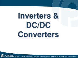
DC/DC Converters with transparent electronics for application on photovoltaic panels. Romano Torres 9th January 2013. DC/DC Converters. To convert a dc input voltage Vs into a dc output voltage Vo; To regulate the dc output voltage against load and line variations;

E N D
DC/DC Converters with transparent electronics for application on photovoltaic panels Romano Torres 9th January 2013
DC/DC Converters • To convert a dc input voltage Vs into a dc output voltage Vo; • To regulate the dc output voltage against load and line variations; • To reduce the ac voltage ripple on the dc output voltage below the required level; • To provide isolation between the input source and the load; From reference [10]
Applications • Electronic devices: • Internal sub-circuits require different voltage levels; • Low battery voltage level needed. • Photovoltaic panels: • Increase the voltage level of electric current produced.
Step-Down Buck Converter Image from reference [10]
Step-Up Boost Converter Image from reference [10]
Buck-Boost Converter Image from reference [10]
Cuk Converter Image from reference [10]
Transparency Resistors Capacitors Images from reference [5]
Transparent thin-film transistors • In 2003 appear the first successful reports of TTFT using ZnO as channel layer material [1] [3] [8]. • In 2004, K. Nomura et al. report the successful fabrication of TTFT with a-GIZO (amorphous gallium-indium-zinc-oxide) [9].
TTFT device structure Staggered bottom-gate Image from reference [10]
TFT operation modes Cut-off: Vgs<Vt No current flow. Pre-saturation: Vgs>Vt& Vds<Vgs-Vt Saturation: Vds>Vgs-Von
a-GIZO TFT limitations • p-type devices with poor semi-conductor characteristics; • Threshold voltage shift due DC-bias; • Source and drain contacts’ resistance influence the TFT characteristics;
a-GIZO TFT limitations • Temperature: • Oxygen vacancy. Image from reference [6]
a-GIZO TFT limitations • Light: Image from reference [7]
Transparency • Problems with inductors: • Poor conductance; • High parasitic resistance; • Low quality factor.
Voltage multipliers • Due the various problems with transparent inductors, we propose use voltage multipliers; • How does it work?
Proposed positive DC/DC Converter Images from reference [4]
Proposed negative DC/DC Converter Images from reference [4]
Transparent photovoltaic panels Image from reference [2]
References • [1] P. F. Carcia, R. S. McLean, M. H. Reilly and G. Nunes, "Transparent ZnO thin-film transistor fabricated by RF magnetron sputtering", Applied Physics Letters, vol.82, no.7, pp. 1117-1119, Feb 2003. • [2] C. Chen, L. Dou, R. Zhu, C. Chung, T. Song, Y. Zheng, S. Hawks, G. Li, P. Weiss, and Y. Yang, “Visibly transparent polymer solar cells produced by solution processing,” in American Chemical Society vol. 6 no.8, 2012, pp. 7185-7190. • [3] R. L. Hoffman, B. J. Norris and J. F. Wager, "ZnO-based transparent thin-film transistors", Applied Physics Letters, vol.82, no.5, pp. 733-735, Feb 2003. • [4] S. Hong, “DC-DC Converters using Indium Gallium Zinc Oxide thin film transistors for mobile display applications,” in Japanese Journal of Applied Physics, 2010. • [5] D. Keszler, R. Presley and J. Wager, Transparent Electronics. New York, USA: Springer, 2008. • [6] S. Kuk, S. Lee, S. Kim, B. Kim, S. Park, J. Kwon, and M. Han, “Light-induced hysteresis of In–Ga–Zn–O thin-film transistors with various temperatures,” in IEEE Electron Device Letters vol. 33 no. 9, 2012, pp. 1279-1281. • [7] S. Lee, S. Kim, Y. Lee, W. Lee, K. Yoon, J. Kwon, and M. Han, “The effect of the photo-induced carriers on the reliability of Oxide TFTs under various intensities of light,” in IEEE Electron Device Letters vol. 33 no. 2, 2012, pp. 218-220. • [8] S. Masuda, K. Kitamura, Y. Okumura, S. Miyatake, H. Tabata and T. Kawai, "Transparent thin film transistors using ZnO as an active channel layer and their electrical properties", Journal of Applied Physics, vol.93, no.3, pp. 1624-1630, Feb 2003. • [9] K. Nomura, H. Ohta, A. Takagi, T. Kamiya, M. Hirano, and H. Hosono, “Room-temperature fabrication of transparent flexible thin-film transistors using amorphous oxide semiconductors,” in Nature vol. 432, 2004,pp.488–492. • [10] M. Rashid, “DC DC Converters,” in Power Electronics Handbook. San Diego, USA: Academic Press, 2001, pp. 211-224.