Download
1 / 30
310 likes | 471 Vues
Laser-structure accelerators. B. Cowan, M.-C. Lin, B. Schwartz, Tech-X Corporation E. Colby, J. England, C. McGuinness , C. Ng, R. Noble, J. Spencer, SLAC R. Byer , Stanford University. Outline. Motivation A tour of structure types Macroscopic structures

E N D
Laser-structure accelerators B. Cowan, M.-C. Lin, B. Schwartz, Tech-X Corporation E. Colby, J. England, C. McGuinness, C. Ng, R. Noble, J. Spencer, SLAC R. Byer, Stanford University
Outline • Motivation • A tour of structure types • Macroscopic structures • Grating-enabled slab structures • Photonic bandgap structures • Laser-structure concepts • Gradient • Efficiency • Beam dynamics • Microfabrication • Ongoing work • Computation • Beam experiments • Injectors
Motivation: Laser-driven acceleration using dielectric structures • High gradient • Take advantage of intense laser fields • High dielectric breakdown thresholds • Efficiency • Laser wall-plug to optical efficiency continues to improve • Optics have low loss • Operate in stable, linear regime • Many concepts carry over from RF • Generate attosecond bunches
Macroscopic structures: Demonstration of microbunching and acceleration Observation of microbunching: Sears et al. PRST-AB 11, 061301 (2008) Free-space accelerating structure Net acceleration: Sears et al. PRST-AB 11, 101301 (2008) Optically bunch the beam in IFEL, follow with accelerating structure First observed by Kimura et al. at ATF with 2 IFELs Net acceleration using linear structuredemonstrated at SLAC Structure used tilted free-space mode
What’s next for structures? • Want to develop scalable structure – accelerate over many Rayleigh lengths • Need to generate axial electric field • Speed-of-light phase velocity for matching to high-energy beam • How do we scale down RF structures to optical wavelengths? • Ideally, use waveguide: Similar to RF, high efficiency • But for index-guiding (as in conventional fiber-optics) fields in vacuum are slow waves: Waveguides get complicated
Courtesy G. Travish At UCLA, we are designing an optical accelerator consisting of a diffractive optic coupling structure and a partial reflector
Courtesy G. Travish A long term goal is to develop a mm-scale, laser-powered, disposable, relativistic particle source MAP: Micro Accelerator Platform
More slab/grating structures Courtesy T. Plettner Slab structures tend to use gratings: Gratings induce phase shifts for matching to a particle beam
Interlude: Photonic bandgaps (PBGs) A photonic crystal is a structure with periodic dielectric constant Like electronic states in solids, EM modes form bands Band gaps can form, in which propagation is prohibited
Benefits of photonic bandgaps Axial field Provide confinement in “defect” — an interruption in the lattice Can confine a speed-of-light mode in all-dielectric structure – impossible with index (total internal reflection) guiding Only confines modes in bandgap frequency range – automatic HOM damping
PBGs with reduced dimension: Fibers Geometry, mode and gap map of fiber structure from X. E. Lin, PRST-AB 4, 051301 (2001) PBGs can be made with periodic structure in some dimensions, uniform in others Ex. PBG fibers: Periodic in transverse dimension; longitudinally uniform Certain dispersion points (ω, kz) are prohibited for all 2D propagation vectors
PBGs: They’re not just for optical structures! Geometry and modes of metallic PBG structure based on triangular transverse lattice. From Smirnovaet al., PRL 95, 074801 (2005) Dielectric Bragg structure, from Jing et al, NIM A 594, 132 (2008) HOM damping motivated PBG structure development in the RF regime
Modeling Photonic Band Gap Fibers and Defect Modes • Goals: • Design fibers to confine vphase = c defect modes within their bandgaps • Understand how to optimize accelerating mode properties: ZC, vgroup, Eacc/Emax ,… • Codes: • RSOFT – commercial photonic fiber code using Fourier transforms • CUDOS – Fourier-Bessel expansion from Univ of Sydney • Accelerating Modes in Photonic Band Gap Fibers • Accelerating modes identified as special type of defect mode called “surface modes”: dispersion relation crosses the vphase=c line and significant field intensity at defect edge. • Tunable by changing details of defect boundary. Modifying Accel. Mode via Defect Radius: Increasing the Accel. Field: Ez of 1.89 µmaccel. mode in Crystal Fibre HC-1550-02 HC-1550-02 Band Gaps Modified X.E. Lin hollow core silica fiber with improved ratio Eacc/Ez matrix obtained by filling the first layer holes with εr = 1.5 material Courtesy R. Noble et al.
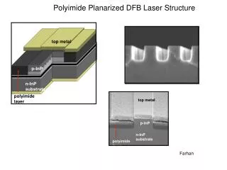
3D “woodpile”-based structure Axial field Si (εr = 12.1) Vacuum PRST-AB 11, 011301 (2008) Has complete bandgap; requires high index Lithographic fabrication can allow incorporation of features, e.g. coupling elements Supports speed-of-light, near-lossless accelerating mode
Key structure concept: Sustainable gradient(Also not just for optical structures!) (For THz measurements see Thompson et al., PRL 100, 214801 (2008)) Si Proc. SPIE 6720, 67201M-1 Stuart et al., PRB 53, 1749 (1996) Simanovskiiet al., PRL 91, 107601 (2003) • One conclusion: Short pulses are good (at least down to~1 ps) • Gradient fundamentally limited by breakdown of material • Huge unexplored territory: What are best parameters? • 5 orders of magnitude in frequency (RF to optical) • Lots of materials • Relatively little data
Woodpile gradient example • Based on damage threshold of bulk silicon, sustainable gradient is 300 MeV/m at λ = 1550 nm, 1 ps pulse width • Could get to 400 MeV/m at longer wavelength; GeV/m challenging in silicon • Higher-bandgap materials could allow higher gradient • Achievable with 500 W peak laser power • Commercially available in fiber systems • Low group velocity laserpulse slips 1 ps relative toparticle beam in 100 μm • Frequent coupling & compactcoupler needed
Optical accelerator efficiency From Y. C. Neil Na et al., PRST-AB 8, 031301 (2005) IFEL + chicane RF electron bunch Optically-bunched beam Bunch charge and optical-to-beam efficiency limited by wakefields Embed accelerator in optical resonator to recycle energy; use multiple bunches Beam can consist of a single optical bunch or a train of optical bunches spaced by λ
Efficiency optimization efficiency charge reflectivity Optimize resonator beamsplitter reflectivity and bunch charge for optimum efficiency Efficiency 37% for single bunch, 76% for 100 bunches Bunch charge ~few fC, so rep rate must be high Energy spread could be problem
Beam dynamics considerations • Two problems ⇒ one solution • Idea: Use the optical structures π/2 out of phase as focusing elements • Adjust waveguide geometry to suppress quadrupole fields during acceleration • Geometry is key Perturb woodpile structure by adjusting central bar Structure has small aperture: 1.55μm× 1.41μm Structure is not azimuthally symmetric has strong transverse focusing and nonlinear forces for off-crest particles
Effect of geometry change Quadrupole field suppressed Focusing mode with octupole field suppressed: ~ 831 kT/m magnet Original mode Into guide Out of guide 2 modes available; suppress quadrupole field in accelerating mode and octupole field in focusing mode We can now use thin lenses
Beam confinement Dynamic aperture, on-crest particles Results for full 6D tracking simulation over 3 m 87% energy gain Emittance requirement: Use accelerating and focusing structures to create thin-lens F0D0 lattice Resulting design has high dynamic aperture, low emittance growth
Computational issues PBG lattice defect • Computing properties of photonic crystal structures is hard • High-order mode • Large computational area • For n “cladding” layers: • Computational cell size ~ n2 • Mode number ~ n2 • Computations can be orders ofmagnitude more intensive than formetal-bounded structures for similar resolution • High-performance computing is beginning to be brought to bear • Advanced dielectric algorithms • Frequency extraction techniques from time-domain simulation
e metal vacuum field emitter tip P. Hommelhoff et al, Kasevich group, Stanford University Field emission tip properties laser beam • laser-assisted tunneling of electrons from the atom to free space • Highly nonlinear • Potential for timed sub-optical cycle electron emission P. Hommelhoff, Y. Sortais, A. Aghajani-Talesh, M. A. Kasevich, “Field Emission Tip as a Nanometer Source of Free Electron Femtosecond Pulses”, PRL 96, 077401 (2006)
Summary • Optical structures hold great promise for laser-driven acceleration • Groundwork in place further exploration • Linear acceleration in vacuum demonstrated • Several structure designs simulated • Efficiency and beam focusing concepts described • Fabrication and experimentation underway • Much work remains to be done and many exciting ideas to explore • Many concepts carry over to other frequency ranges
Acknowledgments Collaborators at SLAC/Stanford J. Rosenzweig, G. Travish (UCLA) A. Chao, A. Wachsmann (SLAC) S. Fan, D. Simanovskii (Stanford) M. Tang (SNF) Work supported by Department of Energy contracts DE-AC02-76SF00515 (SLAC), DE-FG06-97ER41276 (LEAP), and DE-SC0000839 (SBIR), and by Tech-X Corporation. Bob
Diamond structure a w Omnidirectionalbandgap: 5.4% width-to-center ratio Simulate woodpile structure based on diamond: n = 2.395 at λ= 1.55 μm First, optimize the lattice: Adjust rod width w for largest bandgap; optimum at w = 0.37a
Step 2: Compute an accelerating mode Frequency near bandgap edge; loss might be reduced by altering waveguide to bring frequency into the gap For diamond, electronic bandgap is 5.5 eV, requiring 7 absorption for ionization at λ = 1.55μm Mode parameters (with Si structure parameters for comparison):