Download
1 / 23
410 likes | 1.45k Vues
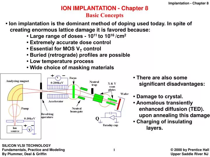
ION IMPLANTATION - Chapter 8 Basic Concepts. • Ion implantation is the dominant method of doping used today. In spite of creating enormous lattice damage it is favored because: • Large range of doses - 10 11 to 10 16 /cm 2 • Extremely accurate dose control

E N D
ION IMPLANTATION - Chapter 8 Basic Concepts • Ion implantation is the dominant method of doping used today. In spite of creating enormous lattice damage it is favored because: • Large range of doses - 1011 to 1016 /cm2 • Extremely accurate dose control • Essential for MOS VT control • Buried (retrograde) profiles are possible • Low temperature process • Wide choice of masking materials • There are also some significant disadvantages: • Damage to crystal. • Anomalous transiently enhanced diffusion (TED). upon annealing this damage. • Charging of insulating layers.
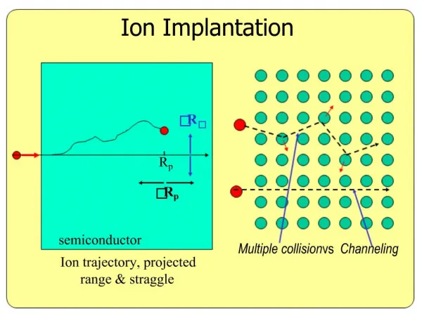
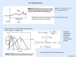
A. Implant Profiles • At its heart ion implantation is a random process. • High energy ions (1-1000keV) bombard the substrate and lose energy through nuclear collisions and electronic drag forces. • Profiles can often be described by a Gaussian distribution, with a projected range and standard deviation. (200keV implants shown.) (1) or (2) where Q is the dose in ions cm-2 and is measured by the integrated beam current.
Ranges and standard deviation ∆Rp of dopants in randomly oriented silicon.
• Monte Carlo simulations of the random trajectories of a group of ions implanted at a spot on the wafer show the 3-D spatial distribution of the ions. (1000 phosphorus ions at 35 keV.) • Side view (below) shows Rp and ∆Rp while the beam direction view shows the lateral straggle.
• The two-dimensional distribution is often assumed to be composed of just the product of the vertical and lateral distributions. (3) • Now consider what happens at a mask edge - if the mask is thick enough to block the implant, the lateral profile under the mask is determined by the lateral straggle. (35keV and 120keV As implants at the edge of a poly gate from Alvis et al.) (Reprinted with permission of J. Vac. Science and Technology.) • The description of the profile at the mask edge is given by a sum of point response Gaussian functions, which leads to an error function distribution under the mask. (See page 7 of class notes on diffusion for a similar analysis.)
B. Masking Implants • How thick does a mask have to be? • For masking, (4) • Calculating the required mask thickness, (5) • The dose that penetrates the mask is given by (6)
C. Profile Evolution During Annealing • Comparing Eqn. (1) with the Gaussian profile from the last set of notes, we see that ∆Rp is equivalent to . Thus (7) • The only other profile we can calculate analytically is when the implanted Gaussian is shallow enough that it can be treated as a delta function and the subsequent anneal can be treated as a one-sided Gaussian. (Recall example in Chapter 7 notes.) (8)
• Real implanted profiles are more complex. • Light ions backscatter to skew the profile up. • Heavy ions scatter deeper. • 4 moment descriptions of these profiles are often used (with tabulated values for these moments). (9) Range: (10) Std. Dev: (11) Skewness: • Real structures may be even more complicated because mask edges or implants are not vertical. (12) Kurtosis:
D. Implants in Real Silicon - Channeling • At least until it is damaged by the implant, Si is a crystalline material. • Channeling can produce unexpectedly deep profiles. • Screen oxides and tilting/rotating the wafer can minimize but not eliminate these effects. (7˚ tilt is common.) • Sometimes a dual Pearson profile description is useful. • Note that the channeling decreases in the high dose implant (green curve) because damage blocks the channels.
Modeling of Range Statistics • The total energy loss during an ion trajectory is given by the sum of nuclear and electronic losses (these can be treated independently). (13) (14) A. Nuclear Stopping • An incident ion scatters off the core charge on an atomic nucleus, modeled to first order by a screened Coulomb scattering potential. (15) • This potential is integrated along the path of the ion to calculate the scattering angle. (Look-up tables are often used in practice.) • Sn(E) in Eqn. (14) can be approximated as shown below where Z1, m1 = ion and Z2, m2 = substrate. (16)
B. Non-Local and Local Electronic Stopping • Drag force caused by charged ion in "sea" of electrons (non-local electronic stopping). • Collisions with electrons around atoms transfers momentum and results in local electronic stopping. (17) • To first order, where C. Total Stopping Power • The critical energy Ec when the nuclear and electronic stopping are equal is B: ≈ 17keV P: ≈ 150keV As, Sb : > 500keV • Thus at high energies, electronic stopping dominates; at low energy, nuclear stopping dominates.
Damage Production • Consider a 30keV arsenic ion, which has a range of 25 nm, traversing roughly 100 atomic planes. (18) • Molecular dynamics simulation of a 5keV Boron ion implanted into silicon [de la Rubia, LLNL]. • Note that some of the damage anneals out between 0.5 and 6 psec (point defects recombining).
Amorphization • For high enough doses, the crystal becomes amorphous and loses all long range order. At this point, the arrangement of lattice atoms is random and the damage accumulation has saturated. • Cross sectional TEM images of amorphous layer formation with increasing implant dose (300keV Si -> Si) [Rozgonyi] • Note that a buried amorphous layer forms first and a substantially higher dose is needed before the amorphous layer extends all the way to the surface. • These ideas suggest preamorphizing the substrate with a Si (or Ge) implant to prevent channeling when dopants are later implanted.
Damage Annealing - Solid Phase Epitaxy • If the substrate is amorphous, it can regrow by SPE. • In the SPE region, all damage is repaired and dopants are activated onto substitutional sites. • Cross sectional TEM images of amorphous layer regrowth at 525˚C, from a 200keV, 6e15 cm-2 Sb implant. • In the tail region, the material is not amorphized. • Damage beyond the a/c interface can nucleate stable, secondary defects and cause transient enhanced diffusion (TED).
Damage Annealing - “+1” Model Goals: • Remove primary damage created by the implant and activate the dopants. • Restore silicon lattice to its perfect crystalline state. • Restore the electron and hole mobility. • Do this without appreciable dopant redistribution. • In regions where SPE does not take place (not amorphized), damage is removed by point defect recombination. • Bulk and surface recombination take place on a short time scale. • "+1" I excess remains. These I coalesce into {311} defects which are stable for longer periods. • {311} defects anneal out in sec to min at moderate temperatures (800 - 1000˚C) but eject I TED.
Dopant Activation • When the substrate is amorphous, SPE provides an ideal way of repairing the damage and activating dopants (except that EOR damage may remain). • At lower implant doses, activation is much more complex because stable defects form. • Plot (above left) of fractional activation versus anneal temperature for boron. • Reverse annealing (above right) is thought to occur because of a competition between the native interstitial point defects and the boron atoms for lattice sites.
Transient Enhanced Diffusion • TED is the result of interstitial damage from the implant enhancing the dopant diffusion for a brief transient period. • It is the dominant effect today that determines junction depths in shallow profiles. • It is anomalous diffusion, because profiles can diffuse more at low temperatures than at high temperatures for the same Dt. • The basic model for TED assumes that all the implant damage recombines rapidly, leaving only 1 interstitial generated per dopant atom when the dopant atom occupies a substitutional site (the +1 model) [Giles]. • TED effects may be very non-local. • After 900˚C, 1 sec anneal, the amorphous As surface profile recrystalizes by SPE without much TED. • The buried boron layer is drastically affected by the +1 interstitials in the As tail region.
Atomic Level Understanding Of TED • {311} clusters form rapidly and then are stable for extended periods (sec - min), driving TED by emitting I while they shrink. • By 0.1 sec (750˚C), the {311} defects have formed and CI is down to ≈ 1013 cm-3 (SUPREM). • But ≈ 108 cm-3 at 750˚C, so the enhancement is > 105! • On a much larger time scale, the {311} clusters decay. • These act as an ongoing source of excess interstitials which drives TED. • TED lasts hours at very low T, minutes at intermediate T and msec at very high T.
• Given this picture, we can model the {311} behavior as follows: (where Cln is a cluster with n interstitials) (19) (20) • The most important part of the transient is while the {311} clusters are evaporating I, maintaining a constant supersaturation of I. • During this period, dopant diffusivity enhancements are ≈ constant and given by (see text): (21) • Note that the diffusivity enhancement is as large as 10,000 at low T and falls off to 100 - 1000 at RTA temperatures. • These calculated values agree with experimental measurements.
Estimating the Duration of TED • Over time the interstitial supersaturation decays to zero and TED ends. • Example - Boron TED (TSUPREM IV). Note that CI/has dropped from 104 to 102 in 10 min at 750˚C. • The excess I diffuse into the bulk and recombine at the surface. • Note the relatively flat interstitial profiles (dashed) except at the surface where recombination is occurring. • The flux towards the surface is where RP is the range of the implant. • The time to dissolve the clusters is given by the dose divided by the flux (see text): (22)
• Plot of Eqn. 22. This matches the experimental data on page 18 of these notes (Fig. 8-33 in text). • Note that TED persists for hours at low T and disappears in msec at very high T. • Thus the general picture of TED that emerges is as shown on the lower left. • Because the {311} clusters exist for much longer times at low T, there can actually be greater dopant motion during low T anneals (below).
• 2D SUPREM simulation of small MOS transistor. • Ion implantation in the S/D regions generates excess I. These diffuse into the channel region pushing boron (channel dopant) up towards the surface. • Effect is more pronounced in smaller devices. • Result is that VTH depends on channel length (the "reverse short channel effect" only recently understood). (See text - Chpt. 7 - for more details on this example.)
Summary of Key Ideas • Ion implantation provides great flexibility and excellent control of implanted dopants. • Since implanted ion energies are >> Si-Si binding energy (≈ 15 eV), many Si lattice atoms are displaced from lattice positions by incoming ions. • This damage accumulates with implanted dose and can completely amorphize the substrate at high doses. • The open structure of the silicon lattice leads to ion channeling and complex as-implanted profiles. • TED is the biggest single problem with ion implantation because it leads to huge enhancements in dopant diffusivity. • Understanding of TED has led to methods to control it (RTA annealing). • Nevertheless, achieving the shallow junctions required by the NTRS will be a challenge in the future since ion implantation appears to be the technology choice.