Download
1 / 11
110 likes | 217 Vues
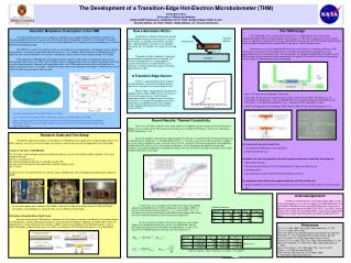
Mo/Au Transition-Edge Hot-Electron Micro-Bolometers. S. Ali , S. Malu , D. McCammon , K. L. Nelms , R. Pathak , P. T. Timbie , D. van der Weide University of Wisconsin-Madison, Madison, WI 53706

E N D
Mo/Au Transition-Edge Hot-Electron Micro-Bolometers S. Ali , S. Malu , D. McCammon , K. L. Nelms , R. Pathak , P. T. Timbie , D. van der Weide University of Wisconsin-Madison, Madison, WI 53706 C.A.Allen, J. Abrahams, J. Chervenak, W.-T. Hsieh, T. M. Miller, H. Moseley, T.R.Stevenson, E.J. Wollack NASA Goddard Space Flight Center, Greenbelt, MD 20771
Abstract We are developing a new type of detector for observational cosmology and astrophysical research. Incoming radiation from the sky is coupled via a planar antenna and superconducting transmission lines to a thin metal film absorber. At sub-Kelvin temperatures the thermal isolation between the electrons and the lattice causes the radiation to selectively heat the electrons in the small absorber. An adjacent superconducting transition-edge sensor (TES) is thermally coupled to the hot electrons and measures their temperature. The volume of the absorber and TES is a few cubic microns. We call this detector Transition-edge Hot-electron Micro-bolometer (THM). We have constructed and tested a scale model of a planar antenna. We have tested the thermal properties of Mo/Au TES devices.
Bismuth Nb microstrip Z ~ 10W Mo leads Mo/Au bilayer GAndreev GAndreev GWF e Superconducting leads e Superconducting leads Gep IRF from antenna e Lattice Phonons Model of a THM The weak electron –phonon link provides the thermal isolation for the hot electron microbolometer. Absorber
Planar Antenna-Coupled THMs THMs can be easily coupled to lithographically fabricated polarization sensitive slot antennas via superconducting micro-strip lines.
Test Device Fabrication THM devices are fabricated by patterning Mo(40nm) /Au (156.5nm) bilayer. 1) Apply Trench mask. Ion mill gold. RIE Mo. 2) Apply TES mask . Ion mill gold. 3) Apply Mo leads mask. RIE Mo. 4) Evaporate 500 nm Bi absorber/heater and pattern by lift-off.
R vs T Curve with Different Bias Currents The test THM is 10 mm x 20 mm x 196.5nm thick. A 10 mm x 100 mm x 500 nm thick Bi absorber covers the TES. The absorber does not “proximitize’ the TES. The transition curve of a TES with an absorber is very similar to that of one without an absorber. Resistance versus temperature curves measured at constant current for the test device show a steep transition ~ 5mK wide. The measurements are made with a shielded ADR.
R vs T curves for the same device with different dc currents through the bismuth absorber/heater The test device TES was biased with a constant ac bias current (0.6 mA) while the absorber was heated by a dc current. The absorber has a resistance of about 2 ohms. A value for G can be calculated from this data which is consistent with the electron-phonon decoupling model.
Simulation for thermal conductance The internal electron electron thermal conductance in the absorber is given by: Gwf= Lo T/Rabs Where, Lo = Lorentz constant T= temperature Rabs = Resistance of the absorber The electron-phonon thermal conductance is given by Ge-ph = 5SVT4 , where S= constant dependent on the absorber material, V= volume of the absorber, and T= temperature.
Estimation of Alpha The R vs. T curves for the test device were taken with constant current bias. But a TES is actually voltage biased when read out by a SQUID. The constant voltage points calculated from the previous constant current bias curves are plotted versus temperature to estimate alpha.
By comparing our data with the electron-phonon thermal conductance model we conclude that there are two separate paths for the heat to get from the hot electrons in the Bi absorber to the substrate 1)e-p interactions in the Bi absorber 2) e-p interactions in the Mo/Au TES. The data suggests that the dominant conduction path to the lattice is through the TES. Calculated electron-phonon conductance Electrical power dissipated in the absorber as a function of the electron temperature(T_tes) and the phonon temperature (T_bath). In these tests, T_tes is constant at T_tes= Tc.
Conclusion • We have measured the R vs T for a small TES device. • Addition of a thick Bi absorber on top of a small TES device does not seem to affect its electrical properties. • The value of thermal conductance calculated from data is consistent with electron-phonon decoupling in both Bi and Mo/Au films. • We plan to measure the device in voltage bias mode shortly. • We have fabricated some 10mm x 10mm Mo/Cu THM devices with Cu absorbers for comparison.