Download
1 / 10
100 likes | 266 Vues
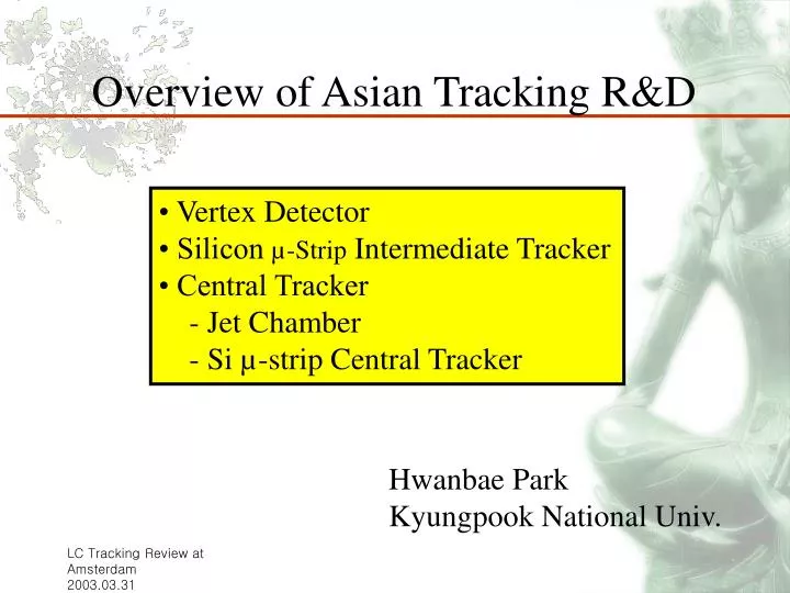
Overview of Asian Tracking R&D. • Vertex Detector • Silicon µ-Strip Intermediate Tracker • Central Tracker - Jet Chamber - Si µ -strip Central Tracker. Hwanbae Park Kyungpook National Univ. ▣ JLC: Tracker. ▣ Vertex Tracker Working Group. • CCD based Vertex Tracker Group

E N D
Overview of Asian Tracking R&D • Vertex Detector • Silicon µ-Strip Intermediate Tracker • Central Tracker - Jet Chamber - Si µ-strip Central Tracker Hwanbae Park Kyungpook National Univ.
▣ Vertex Tracker Working Group • CCD based Vertex Tracker Group Y. Sugimoto*, A. Miyamoto (KEK) N. Tamura, G. Iwai, K. Fujiwara, H. Takayama (Niigate U.) K. Abe, T. Nagamine (Tohoku U.) T. Aso (Toyama National College of Maritime Technology) http://www-jlc.kek.jp/subg/svd/
S/N > 10 @278K Intrinsic Resolution Is better than 3 um. ▣ R&D Activities: Vertex Tracker √ operation at near room temperature √ spatial resolution, S/N ratio √ partially thinned wafers √ radiation hardness √ fast readout
18.5cm 76.5cm ▣ Intermediate Tracker Working Group • SiliconIntermediate Tracker Group H. Park* (Kyungpook National U.) I.H. Park (Ewha Womans U.), B.G. Cheon (SKKU) H.J. Kim, J.H. Kang, Y.J. Kwon (Yonsei U.) J.S. Kang (Korea U.), S. Kim, J. Lee (SNU)
Si Bare Si wafer Oxidation N+ (Diffusion) Photo Lithography UV UV Metal deposition P+ (Implantation) Oxide Etching Photo-resist Strip Mask2 Mask 1 Photo Lithography Metal Etching Photo-resist Strip ▣ R&D Activities: Intermediate Tracker √linking and reconstruction efficiency (Fast Simulation) √ track momentum resolution (Full Simulation) √ Si PIN diode simulation/design/fabrication √S/N ratio measurement and beam test
▣ Central Tracker Working Group • Jet Chamber Si µ-strip M. Kobayashi*, K. Fujii (KEK) M. Iwasaki*, H. Aihara N. Khalatyan (U. of Tsukuba) (U. of Tokyo) A.M. Bacala (MSU), K. Hoshina (TUAT) T. Abe (Nagoya U.),K. Watanabe (Kogakuin U.) http://www-jlc.kek.jp/subg/cdc/
▣ R&D Activities: Jet Chamber • 4.6 m Test Jet Chamber (6 axial and 10 stereo super layers) √ measurements of wire tensions and positions √ cosmic ray tests with a candidate gas mixtures √ space charge effect measurement √ basic chamber studies with “baby” chamber √ spatial and momentum resolution √ two track separation √ wire material studies √ full CDC detector simulator based on Geant4
▣ R&D Activities: Si µ-strip central tracker (with NLC detector parameters) √ Full Simulation Study for detector parameter √ reconstruction efficiency √ momentum resolution √ photon background simulation • - - #hit1 in central • & #VXD hit=5 • - - #hit2 in central • & #VXD hit=5 - - - #hit3 in central - - - #hit=5 in central |cosq|<0.8
▣ Summary □ Vertex Detector - spatial resolution and distortion of thin wafers measured - innermost layer survive more than 3 years under option “A” - radiation damage effect studied □ Intermediate Tracker - fast and full simulation with 5 layers - Si µ-strip R&D proposal submitted (pending) □ Central Tracker - chamber parameters studied with “baby chamber” - track momentum and two track separation - Si µ-strip R&D started (detail simulation studies carried)