Overview of Memory Technologies and Hierarchies in Computing Systems
480 likes | 616 Vues
This overview provides insights into memory technologies and their characteristics throughout computing history. It discusses different memory types, including primary (registers, cache, main) and secondary (external) memories, highlighting speed, capacity, and cost trade-offs. We explore the evolution of memory, from early systems like Univac and magnetic core memory to modern superconductors, and analyze the memory hierarchy's importance for CPU performance. Additionally, we examine factors influencing memory design and organization, emphasizing the balance between access speed and storage capacity.

Overview of Memory Technologies and Hierarchies in Computing Systems
E N D
Presentation Transcript
Memory Part 1
Overview • memory - anything that can hold data • not all forms work the same • affected by several characteristics • technology • Univac - shift reigster (10 words), mercury delay lines. 404 micro sec to detect signals, 202 micro sec access time
1960’s - magnectic core • donut sized ferrite cores, magnetized in 2 directions • core planes, cost millions of dollars • Today, superconductor memories of same size, few hundred dollars
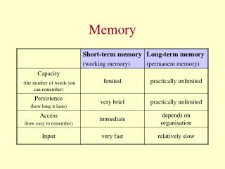
Speed - another memory aspect • faster processor, faster memory requirement • before - 1000 to 2000 ns • Today 8 ns with rates of 40 to 150 ns range, capacity - measured in megabytes
The Memory Hierarchy registers cache Main memory Secondary memory Off-line memory
CPU - registers, highest level • fastest memory in the system • may also have processor main memory • Cache • L1 and L2 cache
Main memory • working memory, also called core memory • electricity alters the “state” of the memory • RAM • 64 M to 512 typically, though can be more
Internal Memory • registers • cache • main memory
External memory • secondary memory • off-line memory • also called auxiliary or mass memory • tapes, floppy's, zip drives, CDs, optical drives, etc • tens to thousands of times larger than main • several hundred gigabytes
Secondary memory • one step away from processor • info for storage must be moved from processor to main memory and then to secondary • info for processing must be taken from secondary to main to processor • almost always electro-mechanical • requires electrical signals and physical movement (disks, tapes, read/write heads etc.) • much, much slower than main memory
Memory Tradeoff • cost, capacity, access time • the faster the access time, higher cost per bit • higher capacity, lower cost per bit • higher capacity, slower the access time • design goal: system with fastest, largest, cheapest memory possible • answer: don’t rely on any single memory technology
Hierarchy progression • cost per bit decreases • capacity increases drastically • access time increases • frequency of access to memory by processor decreases
Balance • rest with the last item • principle of the locality of reference • memory references by processor for both data and instructions will tend to cluster • means that once reference is made to a location during a certain time period, the rest during that time period will be “close” to the first
For main memory, important aspect is to be as fast as possible, but as much as possible • for secondary, important aspect is capacity, but as fast as possible
Example • Suppose that the processor has access to two levels of memory. Level 1 contains 1000 words with an access time of 0.1 s. Level 2 contains 100,000 words with an access time of 1 s. Assume that if a word is to be accessed in Level 1, then the processor accesses it directly. If it is in Level 2, then the word is first transferred to Level 1 and then accessed by the processor. For simplicity, we’ll ignore the time required for the processor to determine if the word is in Level 1 or Level 2. The hit ratio H, is defined as the fraction of all memory accesses that are found in the faster Level 1 memory. Let T1 be the access time for Level 1 and T2 the access time.
If a high percentage of the words required by the processor are in the Level 1 memory, then the average access time will be closer to that of the Level 1 memory than the Level 2 memory. On the other hand if a high percentage of the words required by the processor are located in the Level 2 memory, then the average access time will exceed that of the Level 2 memory. For example, if 95% of all the accesses are found in Level 1 the average access time for all accesses will be: (0.95)(0.1s) + (0.05)(0.1s + 1s) = 0.095 + 0.055 = 0.15s. If the reverse is true and 95% of all accesses are found in Level 2 then the average access time for all accesses will be: (0.05)(0.1s) + (0.95)(0.1s + 1s) = 0.005 + 1.045 = 1.05s.
The overall memory hierarchy makes use of the fact that as you go down the hierarchy less frequent access to that memory portion of the memory will occur.
Characteristics of Memory • .Location of the memory (see the memory hierarchy above). • .Capacity of the memory. • .Unit of transfer into and out of the memory unit. • .Access method. • .Performance parameters such as access time and cycle time.
.Physical type (semiconductor, magnetic, optical, etc.). • .Physical characteristics such as volatile and non-volatile. • .Organization. • Packaging the memory
Capacity • specified in terms of bytes or word • 8, 16, 32, and 64 • External - in terms of bytes • internal - 16 - 512K (or more) • External - several GB (gigabytes) to many TB (terabytes, 1 TB = 240 bytes) or even PB (petabytes, 250 bytes) -- not counting off-line which can be more
Capacity • Library of Congress -- has 1 TB of text characters • One day’s worth of HDTV - 1 TB • A supercomputer references 1PB/day input, output - 1 PB/year • all nonarchival memory will eventually become part of main memory
Unit of Transfer • internal memory -- number of data lines into and out of the module typically • Rambus memory doesn’t follow this model • several issues affect this: • .Word: The “natural” unit of memory organization. The size of the word is typically equal to the number of bits used to represent a number and to the instruction length. There are however, many exceptions. For example, the CRAY-1 has a 64-bit word length but uses 24-bit integer representation. The VAX has a very large number of instruction lengths which are all various multiples of bytes, yet has a word size of 32 bits.
Internal memory issues • .Addressable units: In many systems the addressable unit is the word. However, some systems allow addressing at the byte level. Regardless of which type of addressing is used, the relationship between the length in bits A of an address and the number N of addressable units is 2A = N. • .Unit of transfer: For the main memory, this is the number of bits read out of or written into the memory at a time. The unit of transfer does not need to equal a word or an addressable unit. For external memory, data is often transferred in much larger units than words, typically referred to as blocks.
Access methods • .Sequential access: Memory is organized into units of data, called records. Access must be made in a specific linear sequence. Stored addressing information is used to separate records and assist in the retrieval process. A shared read/write mechanism is used, and this must be moved from its current location to the desired location, passing and rejecting each intermediate record. Thus, the time to access an arbitrary record is highly variable. Tape units are sequential access devices.
Access methods • .Direct access: As with sequential access, direct access involves a shared read/write mechanism. However, individual blocks or records have a unique address based upon their physical location. Access is accomplished by direct access to reach a general vicinity plus sequential searching, counting, or waiting to reach the final location. Again, access time is highly variable. Disk units are direct access.
Access methods • .Random access: Each addressable location in the memory has a unique, physically wired-in addressing mechanism. The time to access a given location is independent of the sequence of prior accesses and is constant. Thus, any location can be selected at random and directly addressed and accessed. Main memory and some cache systems are random access.
Access methods • Associative: This is a random access type of memory that enables one to make a comparison of desired bit locations within a word for a specified match, and to do this for all words simultaneously. Thus, a word is retrieved based on a portion of its contents rather than on its address. As with ordinary random access memory, each location has its own addressing mechanism, and retrieval time is constant and thus independent of location or prior access patterns. Cache memories will typically be the only place where associative memory will be employed.
Performance • 1. Access time: For random access memory, this is the time required to perform a read or write operation. It is the total time from the instant that an address is presented to the memory to the instant that the data has either been stored (write) or made available for use (read). For non-random access memory, this parameter represents the total time taken to position the read-write mechanism at the desired location.
Performance • 2. Memory cycle time: This parameter only applies to random access memory. It is the access time plus any additional time that is required before a second access to the memory can begin. This additional time might be required to allow transients on the signal lines to die out or to regenerate data if the read is a destructive one.
Performance • 3. Transfer rate: This is the rate at which data can be transferred into or out of a memory unit. For random access memory it is equal to the reciprocal of the memory cycle time, i.e., 1/(cycle-time). For non-random access memory, the following relationship will hold:
Performance Tn = Ta + N/R • where: TN = average time to read or write N bits • TA = average access time • N = number of bits transferred • R = transfer rate in bits/second (bps)
Physical Types • internal - semiconductor • external • magnetic surface • also, optical and magneto-optical
Physical Characteristics • 1. Volatility: As with human beings, computers have both short-term (main memory) and long-term (secondary memory) memories. The former are fleeting, the latter are lasting. As far as computer memory is concerned, the reaction it has to an interruption of power defines the difference between long-term and short-term memory. The technical name for this phenomenon is volatility. Computer memory is classified into two distinct categories: volatile and non-volatile. Volatile memory is fast. Non-volatile memory is slow, often much, much slower. PCs built with non-volatile memory while immune to the loss of power would be prohibitively expensive and excruciatingly slow.
Physical Characteristics • i) Volatile memory: The information in the memory cell last only as long as the source of power remains constant. Disconnect the power from the memory cell and the contents will disappear in a few microseconds. The main memory in nearly every PC is volatile. • ii)Non-volatile memory: Information in the memory cell remains there until it is overwritten. Interruption from the power supply does not affect the contents of the memory cell. Read-only-memory (ROM) and flash memory are two common types of non-volatile memory found in modern PCs. Non-volatile memory can be simulated by providing back-up power (usually in the form of a battery). This is commonly done in the CMOS memory configuration memory systems used in most PCs. However, this type of memory will remain vulnerable to the loss of power from the back-up source - if the battery dies - so too does the contents of the memory.
Physical Characteristics • .Erasability: Non-erasable memory cannot be altered, except by destroying the memory unit. Semiconductor memory of this type is known as ROM (Read Only Memory). Practical nonerasable memory must also be non-volatile.
Organization • Basic element of semiconductor memory is the cell • they have two stable (or semi-stable) states, representing 0 or 1 • they are capable of being written (at least once), to set the state • they are capable of being read to sense the state
Organization • cell has three functional units • select - selects memory cell for a read or write • control - indications operation • for writing, remaining terminal carries the signal to set the state • for reading, it carries signal to output the state • inner details of the units depend upon the integrated circuit technology used
Semiconductor memory • a) physical arrangement in W words each B bits wide • b) one-bit-per-chip
DRAM • Dynamic RAM • series of arrays of 2048x2048 cells • connected by row and column lines • rows - connect select terminal of each cell • columns - connect to data-in/sense terminal of each cell • address lines supply the address (total of log W lines) • lines are fed to decoder that activates a single line of outputs, additional lines select columns
1/2 lines come in, but this is passed to select logic which multiplexes the other 1/2 lines needed • Signals accompanied by CAS and RAS signals to provide timing • Refresh - handled by disabling chip while memory cells are refreshed • RESULT- because of multiplexed addressing & square arrays, memory size quadruples with each generation of chips
Chip Packaging • mounted on package with pins for connections • configurations differ
EPROM • Example, 32 pins, 1M x 8 (8M chip) • The address lines of the word being accessed. For 1M words, a total of 20 (220 = 1,048,576 = 1M) pins are needed. These are labeled A0-A19. • The data to be read out (remember it’s a ROM) consists of 8 lines (1 word = 8 bits). These are labeled D0-D7. • The power supply to the chip, labeled VCC. • A ground pin, labeled VSS. • A chip enable pin, labeled CE. Since there may be more than one memory chip connected to the same address bus, the CE pin indicates whether or not the address is valid for this particular chip. The CE pin is activated by logic connected to the higher order bits of the address bus (i.e., address bits above A19). • A program voltage pin, labeled Vpp, that is supplied with the proper voltage during programming (a write operation to a ROM chip).
DRAM • example, 16 M (4M x 4) • data pins are input/output • Write enable (WE) pin, and output enable (OE) pin indicate operation
Module Organization • bit per chip • word per chip • high-ordered interleaved memory • consecutive words lie on same set of chip pairs