Download
1 / 62
620 likes | 879 Vues
Lawrence Berkeley National Laboratory MicroSystems Laboratory. U.S. Department of Energy Detector R&D Review July 8 th , 2009 S. Holland. MSL Overview. The LBNL MicroSystems Lab has facilities and expertise that are unique within the DOE National Laboratories

E N D
Lawrence Berkeley National LaboratoryMicroSystems Laboratory U.S. Department of Energy Detector R&D Review July 8th, 2009 S. Holland
MSL Overview • The LBNL MicroSystems Lab has facilities and expertise that are unique within the DOE National Laboratories • The MSL’s primary mission is the development of advanced detectors for x-ray/UV/visible/near IR imaging, and charged particle detection • The MSL also has production capability for modest-scale sensor fabrication to meet the needs of DOE science projects
Outline • Facilities, Personnel • Advanced CCDs - technology, applications • Major Accomplishments • Beyond HEP - other applications • Future R&D Directions • Conclusion
MSL Facilities • Detector fabrication facility • Class 10 cleanroom completed in 1989 with LBNL General Plant Project (GPP) funds • Originally intended to pursue generic detector R&D for the Superconducting Super Collider • Equipment procurement strategy has been to utilize CMOS production-capable equipment
LBNL MicroSystems Laboratory Class 10 semiconductor fabrication facility Upgraded to 150 mm wafer capability Projection aligner lithography system Beta Squared Lithography (P/E) Atmospheric and low pressure chemical vapor deposition furnaces Expertech (Thermco) Dielectric plasma etcher Lam 4520 XLE
MSL Facilities (cont’) • MSL also includes the CCD Testing Laboratory • 5 test dewars & associated electronics, light projection systems etc • Quantum efficiency test equipment • Pinhole projector for charge diffusion measurement • Class 1000 cleanroom with wirebonder for packaging • Cold probe station for wafer level testing prior to dicing and packaging • Wafer dicing facility
MSL Facilities (cont’) Cold Probe Station: Located in class 1000 clean room Environmental Chamber Dicing Saw QE & charge diffusion testing setup
Additional MSL Infrastructure • CCD mask layout and design rule checking software • Including access to advanced tools used by the IC design group • 2-D semiconductor process and device simulation tools • Absolutely essential for the challenging device-design projects undertaken at the MSL • High-voltage compatible CCDs that can operate at large substrate bias voltages • In progress, R&D on single-photon counting CCDs utilizing hole-initiated impact ionization • Dedicated 8-CPU Linux computer that can run up to 7 process/device simulations simultaneously
MSL Head Count FY09 • MSL Group Leader: N. Roe • Past leaders – H. Spieler, M. Levi, C. Bebek • CCD Design & Processing: • Dr. Steve Holland: device & process design • Nick Palaio: facility manager, process engineer • Guobin Wang: device processing, testing • Co Tran: device processing • CCD Packaging and Testing: • Dr. Bill Kolbe(ret): CCD test & characterization • Julie Lee: CCD testing & cold probing • Armin Karcher: electronics engineer • John Emes: technician (packaging, cold probing) • Yvette Irwin (SSL): part-time technical support • Sharon Jelinsky (SSL): part-time mechanical tech • Postdocs and Students – typically 1-2 of each • The MSL is supported by a combination of KA-15 as well as other sources of funding
Outline • Facilities, Personnel • Advanced CCDs - technology, applications • Major Accomplishments • Beyond HEP - other applications • Future R&D Directions • Conclusion
Scientific CCD overview • Scientific CCDs used in astronomy achieve extraordinary performance, and improvements are still forthcoming • Back illumination to avoid light absorption in the front-side circuitry results in quantum efficiencies approaching 100% • Commercial digital camera imagers peak at ~ 40% • Operation at cryogenic temperatures results in dark currents measured in electrons/pixel-hour, enabling very long exposures to detect faint objects • Slow-scan readout results in read noise levels approaching 1–2 e- rms • Charge transfer inefficiencies less than 1 x 10⁻⁵ allow for CCDs with millions of pixels, without image degradation during readout
Scientific CCD overview (cont’) • In terms of chip size, scientific CCDs are the largest integrated circuits in production • Low fabrication yields for high quality, large format devices still result in relatively high prices • Scientific CCD cameras used in astronomy have enabled significant discoveries for DOE science • Dark Energy: Discovered by the LBNL SCP group who pioneered digital CCD image subtractions to find supernovae • Baryon Acoustic Oscillation: First detected by the Sloan Digital Sky Survey, employing the largest focal plane of its time
Scientific CCD overview (cont’) • The ability to produce Gpixel camera systems is enabling Stage III and Stage IV generation cosmology experiments that complement accelerator-based particle physics (e.g. DES, LSST, JDEM) • Next generation spectroscopy projects are based on advances in QE, read noise (e.g. BOSS, BigBOSS)
ESO OmegaCam European Southern Observatory 32 2k x 4k CCDs 13.5 mm pixels 256 Mpixels Thinned (~ 20 mm) CCDs from e2V The Dark Energy Survey camera will have twice the pixel count, and far better sensitivity in the near infrared
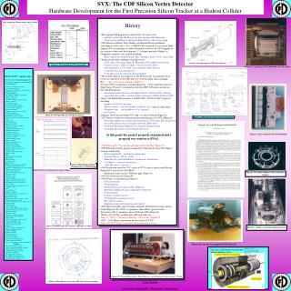
Fully depleted, back-illuminated CCD • 1) Concept: Fabricate a conventional CCD on a thick, high-resistivity silicon substrate • 200-250 µm typical, 675 µm in special cases • 2) Use a substrate bias voltage to fully deplete the substrate of mobile charge carriers • Merging of p-i-n and CCD technology • High-ρ Si allows for low depletion voltages • 3) The thickness results in high near-infrared quantum efficiency and greatly reduced fringing • 4) The fully depleted operation results in the ability to control the spatial resolution via the thickness and the substrate bias voltage • 5) p-channel CCD has vastly improved radiation hardness for space applications
1st CCD developed at LBNL 1st light: 40 kpixel CCD 1st CCD wafer fabricated at LBNL 100 mm wafer, GCA wafer stepper All fabrication done at the MSL except ion implantation (Bay Area vendors) and poly etching (UC-Berkeley campus) S.E. Holland et al, “A 200 x 200 CCD Image Sensor Fabricated on High-Resistivity Silicon”, International Electron Devices Meeting, pp. 911914, December 1996.
Current LBNL CCD efforts on 150 mm diameter wafers with DALSA Semiconductor Dark Energy Survey camera wafer (FNAL) 62 2k x 4k CCDs required for a camera at CTIO telescope in Chile 4k x 4k wafer Sloan/Keck spectrograph upgrades and SWIFT spectrograph (Palomar) SNAP V3 wafer JDEM (space mission) candidate
CCD fabrication We use a hybrid fabrication approach to CCD production We provide CCD designs and wafer layouts Most of the front-side processing is done at DALSA Semiconductor, using technology transferred from LNBL www.dalsa.com 2.5 µm CCD technology with scanner lithography for large-area CCD fabrication 150 mm diameter wafers
CCD fabrication Hybrid fabrication approach to CCD production The wafers are shipped to LBNL after completion of about 80% of the processing The wafers are thinned to the final desired thickness, typically 200–250 µm thick, at a commercial vendor Processing of thinned wafers at the foundry is not feasible at this time, so the specialized steps on thinned wafers necessary to produce back-illuminated CCDs are done at LBNL This is a much more efficient production model than the previous method where all CCD fabrication was done in the MSL However, full production at the MSL was essential in proving the fully depleted CCD concept, and the fabrication experience gained is key to our ability to effectively interface with DALSA Semiconductor
Current deployment of LBNL CCDs MMT 6.5m/Mt. Hopkins Red Channel spectrograph Kitt Peak/Mayall 4m MARS and RC spectrographs Keck 10m LRIS spectrograph Lick Observatory/Mt Hamilton Hamilton Eschelle spectrograph Palomar Hale 200”/SWIFT spectrograph
Future deployments of LBNL CCDs SDSS-III/BOSS 2009 Apache Pt Observatory 2.5 m Dark Energy Survey 2010 CTIO Blanco 4m SNAP/JDEM ?
Outline • Facilities, Personnel • Advanced CCDs - technology, applications • Major Accomplishments • Beyond HEP - other applications • Future R&D Directions • Conclusion
Major Accomplishments • Production of CCDs for the Dark Energy Survey • Delivery of 4k x 4k CCDs for BOSS • Deployment of 2k x 4k CCDs on Keck • Completion of device design and space qualification for SNAP CCDs • CCD technology transfer • Development and delivery of charged particle detectors for the Stereo and Themis space missions
LBNL CCDs for DES • LBNL joined in DES in 2004 (1 of 5 founding inst’s) • Hardware contribution: delivery of the detectors for the 62-CCD focal plane (0.5 billion pixels!) • Responsible for CCD detector design, wafer layout and procurement • Wafers from DALSA are thinned and completed at MSL • Die are cold-probed to identify science grade candidates • Packaging and testing at FNAL SiDET facility • CCD Delivery Status • Delivered 128 pre-production and 252 production 2k x 4k CCDs • Expect to process ~60 more wafers, with 4 CCDs on each wafer • Yield for science-grade candidates is ~25%
Red Sensitivity enables DES Science • DES photometric redshifts out to z~1 require good near-IR sensitivity LBNL fully depleted CCD QE vs conventional CCD DES 5000 sq deg footprint DES filters and elliptical galaxy spectrum at z=0, 0.5, 1
Major Accomplishments • Production of CCDs for the Dark Energy Survey • Delivery of 4k x 4k CCDs for BOSS • Deployment of 2k x 4k CCDs on Keck • Completion of device design and space qualification for SNAP CCDs • CCD technology transfer • Development and delivery of charged particle detectors for the STEREO and THEMIS space missions
SDSS-III: BOSS Spectrograph upgrade • Significant improvement in throughput in the near infrared from use of LBNL CCDs in the red arm; more sensitive to high-z galaxies Fully depleted NIR-sensitive LBNL CCD: improved throughput above 7000A BOSS throughput BOSS – Baryon Oscillation Spectroscopic Survey SDSS throughput
Status of BOSS CCDs • We have fabricated, packaged and tested 2 science grade 4k x 4k CCDs (+ 1 spare) for BOSS • They were installed in the BOSS dewars in May 2009 • First light expected in August 2009
4k x 4k test results at -140C Flat field image (slightly non-uniform light source) Dark current (30 minute exposure) 0.7 electrons/pixel-hour at -140C Science-grade CCD to be installed at the Sloan Digital Sky Survey telescope
Major Accomplishments • Production of CCDs for the Dark Energy Survey • Delivery of 4k x 4k CCDs for BOSS • Deployment of 2k x 4k CCDs on Keck • Completion of device design and space qualification for SNAP CCDs • CCD technology transfer • Development and delivery of charged particle detectors for the STEREO and THEMIS space missions
1st light on Keck LRIS June 6th, 2009 From 8June09 Keck announcement Above is the first exposure taken by the next generation LRIS instrument commissioned on the Keck I telescope June 6, 2009. The test image is of the Whirlpool galaxy, or M51, which is 30 million light years from Earth in the direction of the Canes Venatici constellation. NGC 5195 is seen to the right of the Whirlpool's spiral. The improved LRIS instrument is now the most sensitive moderate-resolution spectrograph in operation. Image credit: WMKO.
Major Accomplishments • Production of CCDs for the Dark Energy Survey • Delivery of 4k x 4k CCDs for BOSS • Deployment of 2k x 4k CCDs on Keck • Completion of device design and space qualification for SNAP CCDs • CCD technology transfer • Development and delivery of charged particle detectors for the STEREO and THEMIS space missions
SNAP Detector R&D • SNAP R&D program started in 2002 after successful Lehman review • One of primary goals was development of space-flight qualified CCDs with high sensitivity in near-infrared, good radiation tolerance and excellent spatial resolution for weak lensing studies • The SNAP CCDs developed by MSL have met all of these requirements and are in the final stages of flight qualification • Packaging of SNAP CCDs was developed in collaboration with Yale University and FNAL SiDET
SNAP Detector R&D • LBNL p-channel technology significantly more resistant to the effects of space protons when compared to the conventional n-channel CCDs • Not planned, a fortuitous side-effect from the early SSC detector development days when we observed that making detectors with low dark current was much easier on high-resistivity n-type silicon • N-channel CCDs degrade due to the generation of phosphorus-vacancy defects that are efficient electron traps • Degrade charge transfer efficiency • For p-channel CCDs the dominant trap is the 2nd order divacancy
Radiation tolerance of SNAP CCDs Proton irradiations performed at the LBNL 88” Cyclotron K. Dawson et al, IEEE Trans. Nucl. Sci., 55, 1725, 2008
SNAP Detector R&D • In order to develop CCDs with sufficiently small point-spread function (PSF, aka spatial resolution), it was necessary to embark on a major device design R&D effort to realize CCDs that can be operated at high substrate bias voltages • 200 µm thick SNAP CCDs have been successfully operated at 200V Test pattern image taken on 12.3 Mpixel SNAP CCD at -140C and 206V substrate bias
Electric Field Electric Field y y Depleted Depleted Undepleted Depletion edge Depletion edge Point source illumination Point source illumination SNAP CCD spatial resolution Response to point-source illumination x-y axis: pixel number z axis; arbitrary units 1100 x 800 back-illuminated CCD, 15 um pixels
PSF measurements on 200 and 280 mm thick CCDs J. Fairfield et al, IEEE Trans. Nucl. Sci., 53, 3877, 2006
SNAP Detector R&D • We are developing with DALSA Semiconductor a process flow that utilizes a refractory metal stack in place of the aluminum • Alternating layers of Ti and TiN • The order of the present process flow is; ~ 80% processing at DALSA, thinning, backside contact formation at 600–650C, contact mask/etch, aluminum metallization, anti-reflecting (AR) coatings • Al not compatible with 600C process steps • The refractory metal process flow is; full completion at DALSA, thinning, backside contact formation at 600–650C, AR coatings • Potential advantages • Simpler process, less costly • Possibility of thinner detectors for improved charge diffusion • Less wafer handling reducing the incidence of “back-side defects” • Main drawback is higher sheet resistance of Ti/TiN compared to aluminum (~ 10x)
SNAP Detector R&D 125 µm thick Ti/TiN wafer
Major Accomplishments • Production of CCDs for the Dark Energy Survey • Delivery of 4k x 4k CCDs for BOSS • Deployment of 2k x 4k CCDs on Keck • Completion of device design and space qualification for SNAP CCDs • CCD technology transfer • Development and delivery of charged particle detectors for the STEREO and THEMIS space missions
Tranfer of CCD technology to industry CCD technology transfer to industry is underway Preferred method is through licensing of LBNL patents U.S. Patent 6,025,585, “Low-resistivity photon-transparent window attached to photo-sensitive silicon detector,” Feb. 15, 2000. U.S. Patent 6,259,085, “Fully depleted back illuminated CCD,'' July 10th, 2001. U.S. Patent 7,271,468 B2, “High-voltage compatible, full-depleted CCD,” Sept. 18, 2007. Patent 6,025,585 has been licensed successfully to Digirad Corporation, a supplier of solid-state gamma cameras for nuclear medical imaging applications – http://www.digirad.com High QE, low dark current LBNL back-illuminated photodiode arrays are a key technology in the portable SPECT gamma-ray camera developed by Digirad Main application is cardiology Also an enabling technology for the charged-particle detectors developed for space missions that are described later
Tranfer of CCD technology to industry CCD technology transfer to industry is underway (cont’) Detailed discussions were held with engineers from Fairchild Imaging However, Fairchild chose to close their CCD fabrication facility and to go with a foundry business model The less preferable technology transfer method, albeit the method that is working, is via LBNL publications and presentations Hamamatsu is producing fully depleted, back-illuminated, p-channel CCDs for the Subaru telescope and for x-ray astronomy groups e2V has described efforts in fully depleted CCD fabrication MIT Lincoln Laboratory is producing 75 µm thick fully depleted CCDs for Pan-STARRS
Major Accomplishments • Production of CCDs for the Dark Energy Survey • Delivery of 4k x 4k CCDs for BOSS • Deployment of 2k x 4k CCDs on Keck • Completion of device design and space qualification for SNAP CCDs • CCD technology transfer • Development and delivery of charged particle detectors for the STEREO and THEMIS space missions
MSL detectors on NASA space missions • Charged particle detectors fabricated in the MSL by Craig Tindall and Nick Palaio in collaboration with the UC-Berkeley Space Sciences Laboratory • STEREO – Studying the Sun in 3D • Supra-Thermal Electron Instrument (STE) on STEREO uses MSL charged particle detectors with improved low-energy detection • ~ 10x improvement over previous MCP-based detectors • 14 detectors delivered for flight and spares http://www.nasa.gov/mission_pages/stereo/main/index.html
Thin backside n+ ohmic contact development ISDP – in-situ doped polysilicon • The thin backside n+ contact technology • developed at the MSL is an enabling • technology for • Photodiodes for medical applications • CCDs • Charged-particle detectors in space SIMS depth profile
MSL detectors on NASA space missions • Charged particle detectors fabricated in the MSL by Craig Tindall • THEMIS – Understanding space weather • Solid State Telescopes (two for ions, two for electrons per spacecraft) • 104 detectors delivered, 80 used in flight THEMIS PIN Diode Fabricated in the MSL http://www.nasa.gov/mission_pages/themis/spacecraft/SST.html
Major Accomplishments (cont’) • Publications: over 30 published papers, regular conference contributions (see complete list at www-ccd.lbl.gov) • Training of students and postdocs • Students: Julie Lundy, Jessamyn Fairfield, Juhi Saha, Koki Takasaki, Joanne Daniels, Jon Thacker, Ingo Grosshans, Timo Foerschler, Jochen Reith, Martin Kreis, Maximilian Fabricius, Markus Redelstab, Jens Steckert, Sebastian Kurz, Heiko Bertsch, Martin Wagner • Two of our former students are in Physics Ph.D programs (Fairfield and Fabricius) • Postdocs: Val Prasad, Stephen Bailey, Kyle Dawson, Nick Mostek • Note that the model for Postdocs has been to split time between MSL efforts and science work with the SuperNova Cosmology Group
Outline • Facilities, Personnel • Advanced CCDs - technology, applications • Major Accomplishments • Beyond HEP - other applications • Future R&D Directions • Conclusion