Download
1 / 1
10 likes | 80 Vues
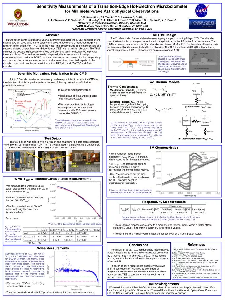
W + P BIAS. TES/ Absorber. T c. G e-p. T bath. W. P BIAS. G e-e. TES/ Absorber. T c. T abs. Absorber. G e-pabs. G e-pTES/abs. T bath. Sensitivity Measurements of a Transition-Edge Hot-Electron Microbolometer for Millimeter-wave Astrophysical Observations

E N D
W +PBIAS TES/ Absorber Tc Ge-p Tbath W PBIAS Ge-e TES/ Absorber Tc Tabs Absorber Ge-pabs Ge-pTES/abs Tbath Sensitivity Measurements of a Transition-Edge Hot-Electron Microbolometer for Millimeter-wave Astrophysical Observations E.M. Barrentinea, P.T. Timbiea, T. R. Stevensonb, S. Alic, J. A. Chervenakb, E. Wollackb, S. H. Moseleyb, C. A. Allenb, W.T. Hseihb, T. M. Millerb, D. J. Benfordb, A. D. Brownb aUniversity of Wisconsin-Madison, Madison, WI 53706 USA bNASA Goddard Space Flight Center, Greenbelt, MD 20771 USA cLawrence Livermore National Laboratory, Livermore, CA 94550 USA Abstract Future experiments to probe the Cosmic Microwave Background (CMB) polarization will need arrays of 1000s of sensitive bolometers. We are developing a Transition-Edge Hot-Electron Micro-Bolometer (THM) to fill this need. This small volume bolometer consists of a superconducting bilayer Transition-Edge Sensor (TES) with a thin film absorber. The THM employs the decoupling between electrons and phonons at mK temperatures to provide thermal isolation. The devices are easily integrated with antennas via microstrip transmission lines, and with SQUID readouts. We present the results of noise, responsivity, and thermal conductance measurements in which electrical power is dissipated in the absorber, and confirm a thermal model for a test THM with a Mo/Au TES and Bi/Au absorber. The THM Design The THM consists of a metal absorber overlapping a superconducting bilayer TES. The absorber forms the termination of a superconducting microstripline that carries RF power from an antenna. The THM test device consists of a thin Bi/Au absorber and bilayer Mo/Au TES. For these tests the microstrip line is replaced by Mo leads attached to the absorber. The TES transitions at 310-317 mK and has a normal resistance of 0.32 Ω. The absorber has a resistance of 17 Ω. (a) Diagram of microstrip-coupled THM. (b) SEM image showing the THM test device. The absorber Bi layer is 500 nm under a 190 nm Au layer. The TES is 40 nm Mo under a 150 nm Au layer. Scientific Motivation: Polarization in the CMB A 0.1uK B-mode polarization anisotropy has been predicted to exist in the CMB and the detection of such a signal would confirm one of the key predictions of inflation, gravitational waves.1 (a) (b) Two Thermal Models Thermal Conductances: Weidemann-Franz, Ge-e: Thermal energy is carried by electrons (or quasiparticles).8 Electron-Phonon, Ge-p: At low temperatures significant decoupling between electrons and phonons. G proportional to volume, V, and Σ, a material dependent constant.7 • To detect B-mode polarization: • Need arrays of thousands of photon-noise-limited detectors. • The most promising technologies include planar antenna-coupled bolometers with TES thermometers read out by SQUIDs.2 Temperature Temperature/E-mode Correlation (a) Ideal Model: Ge-p < Ge-e E-Mode The most recent power spectrum results from WMAP3. An array of THMs would have the sensitivity to reach the predicted B-Mode signal level shown in blue. B-Mode (a) Thermal model for ideal THM. W is power incident on the absorber, PBIAS is Joule power due to the voltage bias of the TES, Tc is the operating temperature for the TES, and Tbath is the cold stage temperature. (b) Thermal model for thermally disconnected THM. The ends of the absorber are at temperature Tabs, while the TES and the absorber nearby the TES are at Tc. Test Setup The test device was placed within a Nb can and heat sunk to a cold stage cooled to ~180-300 mK using a shielded ADR. The TES was placed in parallel with a shunt resistor, RS=25 mΩ, and read out by a NIST 2-stage SQUID with M~190 pH. (b) Disconnected Model: Ge-p > Ge-e I-V Characteristics • In the transition, Joule power dissipation (PBIAS=IVBIAS) is constant, which accounts for the negative slope. • For Tbath~Tc, the transition current decreases and the I-V curve approaches the normal linear regime. • The I-V curves maps out the bias points in the transition. Voltage biasing the TES provides negative electrothermal feedback4 . . THM NIST SQUID W vs. Tbath & Thermal Conductance Measurements • We measured the amount of Joule power dissipated in the absorber, W, at Tc as a function of Tbath. • The disconnected model provides the best fit to W(Tbath). • The disconnected model fits to Σ values only slightly lower than literature values. • Ge-p > Ge-e ,. I-V curves at different cold stage temperatures. The black line indicates the normal resistance. Responsivity Measurements Measured and predicted responsivity (following the block diagram method5) for both thermal models with fitted and literature Σ values (Table 1) for W < 3.5x10⁻¹⁰ W. W vs Tbath fit to disconnected (blue) and ideal (red) model. • The measured responsivities agree to a disconnected thermal model within a factor of 2 for literature values, and within a factor of 2-5 for fitted values. • The ideal thermal model overestimates the responsivity by a much greater factor. ΣBi, ΣAu & G’s (at 310 mK) resulting from fits to W vs. Tbath for the disconnected and ideal models and literature values. *For Rabs=17 Ω. References 1. W. Hu and S. Dodelson, Annu. Rev. Astron. And Astrophys. 40, 171 (2002). 2. Task Force on CMB Research, Final Report, http://www.nsf.gov/mps/ast/tfcr.jsp (2005). 3. Page, L. et al., astro-ph/0603450, (2006). 4. K. D. Irwin, Appl. Phys. Lett. 66, 1998 (1995). 5. M. Galeazzi and D. McCammon, J. Appl. Phys., 93, 4856 (2003). 6. F. C. Wellstood, C. Urbina, and J. Clarke, Appl. Phys. Lett. 54, 2599 (1989). 7. F. Pobell, Matter and Methods at Low Temperature, 2nd Ed., Springer, Berlin-Heidelberg, 64 (1996). 8. F. Pierre, A. B. Gougam, A. Anthore, H. Pothier, D. Esteve, and N. Birge, PRB, 68, 085413 (2003). 9. S. I. Dorozhkin, F. Lell, and W. Schoepe, Solid State Commun., 60, 245, (1986). 10. W.S. Boyle and K.F.Rodgers, J. Opt. Soc. Am.,49, 66 (1959). Conclusions The results of W vs. Tbath, conductance, responsivity & noise measurements for this THM test device are fit well by a thermal model in which Ge-e < Ge-p. These results also agree with literature values for the e-p conductance of Au and Bi. To reach phonon noise-limited sensitivity levels we plan to decrease the THM area by two orders of magnitude and optimize the relative dimensions of the absorber and TES to operate within the ideal thermal model for this detector. Noise Measurements NEP measurements at Tbath= 311 mK for VBIAS = 1 V with predicted noise levels for SQUID, Johnson and thermal noise contributions for the disconnected thermal model with fitted (green) and literature (red) values and the ideal thermal model (purple). For these we followed the block diagram method5, assumed a radiative limit for the thermal noise contributions10 and used the measured responsivity. Acknowledgements We would like to thank Dan McCammon and Mark Lindeman for their helpful discussions and Kent Irwin for providing the SQUID readouts. EB would like to thank the Wisconsin Space Grant Consortium and the NASA-Goddard Graduate Student Research Program for support. • We measure at various TES biases. • The disconnected model with fit Σ provides the best fit to the noise measurements.


![How useful are our measurements? [resolution, signal/noise] Eric](https://cdn1.slideserve.com/2412246/slide1-dt.jpg)