Download
1 / 38
440 likes | 596 Vues
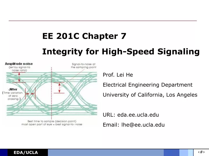
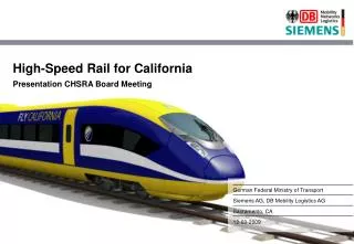
Prof. Lei He Electrical Engineering Department University of California, Los Angeles URL: eda.ee.ucla.edu Email: lhe@ee.ucla.edu. EE 201C Chapter 7 Integrity for High-Speed Signaling. High-speed Links are Everywhere. Backbone Router Rack. PC or Console. [Sredojevic:ICCAD’08].

E N D
Prof. Lei He Electrical Engineering Department University of California, Los Angeles URL: eda.ee.ucla.edu Email: lhe@ee.ucla.edu EE 201C Chapter 7Integrity for High-Speed Signaling
High-speed Links are Everywhere Backbone Router Rack PC or Console [Sredojevic:ICCAD’08]
High-Speed Links: Applications • Chip-to-chip signaling • Computers, games: SDRAM(DDR, DDR2) 100-700MHZ, RDRAM 800-1600MHz, DDR3 800-1600MHz, DDR4 1.6-3.2GHz, XDR DRAM 3.2-6.4GHz • Board-to-board • Computers: Peripherals- PCI (66-133-400MHz), PCIe (250M-500M-1GHz), Infiniband (2.5Gb/s) • Networks • LAN: Fast Ethernet, Gigabit Ethernet, 10G Ethernet • WAN: OC-12 (625MHz), OC-192(12.5GHz) • Routers: 625Mb/s – 2.5Gb/s
Outline Link Design Basics Signal Integrity High Speed Signaling Architectures Equalization
Noise • Signals may be corrupted from many sources • Inter-symbol interference (ISI) • Frequency-dependent attenuation (dispersion) • Reflection • Oscillation • Crosstalk • Power supply noise • Real noise • Thermal and shot noise • Parameter variation • Noise measure • Eye diagram • Timing jitter • Amplitude noise
Inter-Symbol Interference • A signal interfering with itself • Ideally a transmission system is time invariant • No history of previous bits • In reality, the state of the system is affected by previous bits • Signals that don’t reach the rails by the end of cycle • Signal’s transition time is limited by channel bandwidth • Reflections on the transmission lines • Magnitude and phase of excited resonances
ISI - Dispersion • Frequency-dependent attenuation • In general, channel is low pass • Our nice short pulse gets spread out • Example: a 101 pattern
ISI - Reflection • Reflections of previous bits travel up and down transmission lines • A mismatch of δ gives (to the first order) a reflection of ρ
ISI - Resonances • Oscillations are excited by signal transitions and may interfere with later transitions • Excitation of resonant circuits is reduced with longer transition times • Slower edge has less high frequency spectral content • Resistance damps oscillation
Crosstalk • Crosstalk is the coupling of energy from one line to another via: • Mutual capacitance (electric field) • Mutual inductance (magnetic field) • One signal interfering with another signal Mutual Inductance, Lm Mutual Capacitance, Cm Zo Zo Zo Zo far far Cm Lm near Zs near Zs Zo Zo
Crosstalk Induced Noise • The mutual inductance will induce current on the victim line opposite of the driving current (Lenz’s Law) • The mutual capacitance will pass current through the mutual capacitance that flows in both directions on the victim line Zo Zo Zo Zo far far ICm ILm Lm near near Zs Zs Zo Zo
Voltage Profile of Coupled Noise • Near end crosstalk is always positive • Currents from Lm and Cm always add and flow into the node • For PCB’s, the far end crosstalk is “usually” negative • Current due to Lm larger than current due to Cm • Note that far and crosstalk can be positive Zo Zo Far End Driven Line Un-driven Line “victim” Zs Near End Driver Zo
Time = 0 Near end crosstalk pulse at T=0 (Inear) ~Tr V Near end crosstalk Zo TD Far end crosstalk pulse at T=0 (Ifar) ~Tr Time= 1/2 TD 2TD V Zo far end crosstalk Zo Time= TD Far end of current terminated at T=TD V Zo Zo Time = 2TD Near end current terminated at T=2TD V Zo Zo Graphical Explanation
Power Supply Noise • The power supply network has parasitic elements • On-chip: resistive • Off-chip: inductive • Current draw across these elements induces a noise voltage: • Instantaneous current is what matters • May be many times the DC current • 10W chip draws 4A at 2.5V • Peak current may be 10-20A
Simultaneous Switching Outputs (SSO) • When several outputs switch simultaneously, significant current is drawn from the supply or sent into ground • Supply connections have inductance • SSO currents produce a voltage drop across these inductances • On-chip, the VDD to VSS voltage difference decreases • Effect grows with number of drivers switching • Quadratic with the inverse of transition time • Between chips, the drops across VSS inductances can effect driver timing and shift the receiver threshold
Other Noise Sources • Alpha particles • 5MeV particle injects 730fC of charge into substrate • One node typically collects less than 50fC • Thermal and shot noise • Proportional to bandwidth – typically in the uV • Parameter mismatch • VT and β have deviation proportional to 1/sqrt(WL) • Systematic variations depend on layout
Eye Diagram This is a “1” This is a “0” Eye – space between 1 and 0 With voltage noise With timing noise With both!!
Eye Diagram (cont’d) Standard measure for signaling Synchronized superposition of all possible realizations of the signal viewed within a particular interval Timing jitter Deviation of the zero-crossing from its ideal occurrence time Amplitude noise Set by signal-to-noise ratio (SNR) The amount of noise at the sampling time
Outline Link Design Basics Signal Integrity High Speed Signaling Architectures Equalization
Signaling – Main Idea • A good signaling system isolates the signal from noise rather than trying to overpower the noise • Crosstalk • Terminate both ends, use homogeneous media • ISI • Matched terminations, no resonators, rise-time control • Power supply noise • Avoid coupling into signal or reference • Differential signaling • Current mode • stable reference
Signaling Architecture Tradeoffs • Signal modulation • PAM (Pulse-amplitude modulation) • Pulsed (Return-to-Zero, RZ) signaling • Binary (ex:NRZ) or Multiple-level signaling (MLS) • Uni-directional or Bidirectional • Time-multiplexed bidirectional or simultaneous bidir. • Single-ended or differential • Current mode or voltage mode • Bus or single-trace • Point-to-point or multi-drop
Voltage Mode vs Current Mode • Main differences are • Ease of control and generation • Much easier to generate a small current than a small voltage • Coupling of supply noise • 50% of supply noise shows up on the data line in the matched voltage mode; potentially much less in a high-Z current-mode driver • Generation of high-Z switches easier than controlled-Z switches
Single-ended vs Differential • Single-ended signaling • compare to shared reference • Often used with a bus • Issues • Generates SSO noise • How to make reference • How to quiet reference • Crosstalk cannot be made common-mode • Differential signaling • compare between two lines • Noise immunity • Many noise sources become common mode • Issues • Differential must run > 2x as fast as single-ended to make sense • Otherwise, powerx2, pinsx2
Binary vs Multiple-level (4-PAM) • 4-PAM uses 4-levels to send 2 bits per symbol • Each level has 2 bit value • Signaling rate = 4xNyquist • Binary (NRZ) is 2-PAM • Use 2-levels to send one-bit per symbol • Signaling rate = 2xNyquist
Simultaneous Bidirectional Signaling • Wires can transmit waves in both directions • It seems a shame to only use one direction at a time • Simultaneous Bidirectional Signaling • Transmit waves in both directions at the same time • Waveform on wire is superposition of forward and reverse traveling wave • Subtract transmitted wave at each end to recover received wave • There are 3-levels on the line but it’s still 2-level signaling • Much more sensitive to reflections and crosstalk
Output Drivers • Single-ended • SSTL (Stub Series Terminated Logic) • RSL (Rambus Signaling Logic) • GTL (Gunning Transceiver Logic) • Differential • LVDS (Low Voltage Differential Signaling) • CML (Current Mode Logic)
SSTL • Center-terminated, push-pull • Very flexible termination • Allows double, single, or no termination • But source term slows edge rates & limits speed • Very simple • Driver can be simple inverter • Receiver can be simple inverter • But PVT varying output driver means reflections
RSL • Open drain current-source driver • Current-control to keep constant I over PVT • Slew-rate control to keep rate low enough to avoid overshoot & ringing • Low-swing with reference • Relatively expensive and complicated
GTL • Just like Rambus” • But… output driver goes linear • No current-control
LVDS • Differential • Eliminates non-common mode reference noise • Also (ideally) keeps current at driver constant • Termination at the RX on-chip or off-chip • No references, can ship across cable • Requires very wide CM range from RX • Unterminated at driver; reflections occur from discontinuities • Timing of driver push-pull ckt can be a challenge
CML • Open-drain • High common-mode keeps saturation • DC or AC coupled • AC-coupling requires 8b10b coding • Termination • DC-term: Better control of CM than LVDS • Double-terminated • Minimize reflections off driver • Driver and receiver both see 25Ω • More power • 4x LVDS just from 100 Ω -> 25 Ω termination
Outline Link Design Basics Signal Integrity High Speed Signaling Architectures Equalization
Equalization • Channel is band-limited, most of them are low-pass • Goal is to flatten the overall response • Equalization: Boost higher frequencies relative to lower frequencies • Can be done at Tx or RX or both equalizer channel
Receiver Linear Equalizer • Amplifies high-frequencies attenuated by the channel • Pre-decision • Digital or Analog FIR filter • Issues • Also amplifies noise! • Precision • Tuning delays (if analog) • Setting coefficients • Adaptive algorithms such as LMS
Transmitter Linear Equalizer • Tx Pre-emphasis Filter • Attenuates low-frequencies • Need to be careful about output amplitude - limited output power • If you could make bigger swings, you would • EQ really attenuates low-frequencies to match high frequencies • Also FIR filter: D/A converter • Can get better precision than RX • Issues • How to set EQ weights? • Doesn’t help loss at high f


![EE 201C Homework 4 [Due on Feb 26, 2013]](https://cdn5.slideserve.com/9601754/ee-201c-homework-4-due-on-feb-26-2013-dt.jpg)