Download
1 / 18
180 likes | 366 Vues
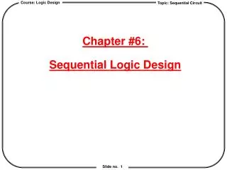
Chapter #6: Sequential Logic Design. Chapter Overview. • Sequential Networks Simple Circuits with Feedback R-S Latch J-K Flipflop Edge-Triggered Flipflops • Realizing Circuits with Flipflops Choosing a FF Type Characteristic Equations

E N D
Chapter Overview • Sequential Networks Simple Circuits with Feedback R-S Latch J-K Flipflop Edge-Triggered Flipflops • Realizing Circuits with Flipflops Choosing a FF Type Characteristic Equations Conversion Among Types • Metastability and Asynchronous Inputs
Sequential Switching Networks Definition of Terms Clock: Periodic Event, causes state of memory element to change rising edge, falling edge, high level, low level Setup Time (Tsu) Minimum time before the clocking event by which the input must be stable There is a timing "window" around the clocking event during which the input must remain stable and unchanged in order to be recognized Hold Time (Th) Minimum time after the clocking event during which the input must remain stable
R Q S R S Q \ Q Sequential Switching Networks Cross-Coupled NOR Gates R S \Q Timing Waveform 100 Reset Hold Reset Set Race Set Forbidden State Forbidden State
Sequential Switching Networks State Behavior of R-S Latch Truth Table Summary of R-S Latch Behavior
Sequential Switching Elements R-S Latch Truth Table: Next State = F(S, R, Current State) Derived K-Map: S(t) R(t) Q(t) Q(t+) 0 0 0 0 (hold) 0 0 1 1 (Hold) 0 1 0 0 (reset) 0 1 1 0 (reset) 1 0 0 1 (set) 1 0 1 1 (set) 1 1 0 Not allowed 1 1 1 Not allowed Characteristic Equation: Q+ = S + R Q t S R-S Latch Q+ R Q
\ Q Sequential Switching Networks J-K Latch J, K both one yields toggle J Q K J(t) K(t) Q(t) Q(t+) 0 0 0 0 (hold) 0 0 1 1 (Hold) 0 1 0 0 (reset) 0 1 1 0 (reset) 1 0 0 1 (set) 1 0 1 1 (set) 1 1 0 1 (toggle) 1 1 1 0 (toggle) J-K Latch Characteristic Equation: Q+ = Q K + Q J
Sequential Switching Networks J-K Latch: Race Condition Reset Set Toggle Race Condition
7474 D Q Clk Positive edge-triggered flip-flop Bubble here for negative edge triggered device Sequential Switching Networks D-FlipFlop Edge triggered device sample inputs on the event edge
Sequential Switching Networks Positive vs. Negative Edge Triggered Devices Positive Edge Triggered Inputs sampled on rising edge Outputs change after rising edge Negative Edge Triggered Inputs sampled on falling edge Outputs change after falling edge Toggle Flipflop Formed from J-K with both inputs wired together
Timing Methodologies Cascaded Flipflops and Setup/Hold/Propagation Delays Shift Register S,R are preset, preclear New value to first stage while second stage obtains current value of first stage Correct Operation, assuming positive edge triggered FF
D-latch and D-Flipflop Transparent latches sample inputs as long as the clock is asserted Example: to be done during the class
Realizing Circuits with Different Kinds of FFs Choosing a Flipflop R-S Clocked Latch: used as storage element in narrow width clocked systems its use is not recommended! however, fundamental building block of other flipflop types J-K Flipflop: versatile building block can be used to implement D and T FFs usually requires least amount of logic to implement ƒ(In,Q,Q+) but has two inputs with increased wiring complexity D Flipflop: minimizes wires, much preferred in VLSI technologies simplest design technique best choice for storage registers T Flipflops: don't really exist, constructed from J-K FFs usually best choice for implementing counters Preset and Clear inputs highly desirable!!
Q J Q C D K Q D implemented with J-K Realizing Circuits with Different Kinds of Flipflops Characteristic Equations R-S: D: J-K: T: Q+ = S + R Q Q+ = D Q+ = J Q + K Q Q+ = T Q + T Q Derived from the K-maps for Q+ = ƒ(Inputs, Q) E.g., J=K=0, then Q+ = Q J=1, K=0, then Q+ = 1 J=0, K=1, then Q+ = 0 J=1, K=1, then Q+ = Q Implementing One FF in Terms of Another
Realizing Circuits with Different Kinds of Flipflops Design Procedure Excitation Tables: What are the necessary inputs to cause a particular kind of change in state?
Metastability and Asynchronous Inputs Terms and Definitions Clocked synchronous circuits • common reference signal called the clock • state of the circuit changes in relation to this clock signal Asynchronous circuits • inputs, state, and outputs sampled or changed independent of a common reference signal R-S latch is asynchronous, J-K FF is synchronous Synchronous inputs • active only when the clock edge or level is active Asynchronous inputs • take effect immediately, without consideration of the clock
Metastability and Asynchronous Inputs Asynchronous Inputs Are Dangerous! Since they take effect immediately, glitches can be disastrous Synchronous inputs are greatly preferred! But sometimes, asynchronous inputs cannot be avoided e.g., reset signal
Chapter Summary • Fundamental Building Block of Circuits with State: latch and flipflop • R-S Latch, J-K Flipflop, Edge-triggered D Flipflop