Download
1 / 21
210 likes | 368 Vues
TBD. FERMI ELETTRA. The Matrix Card and its Applications. 23.09.2009 Dr. John Jones Princeton University neutrinodeathray@gmail.com. CMS CERN. Progression in Physics Hardware Over ~20 Years. Speed. Connectivity. Density. Size. 1995 VME. 2003 VME / ATCA. 2008+ ATCA / μ TCA.

E N D
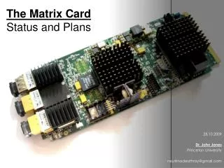
TBD FERMI ELETTRA The Matrix Card and its Applications 23.09.2009 Dr. John Jones Princeton University neutrinodeathray@gmail.com CMS CERN
Progression in Physics Hardware Over ~20 Years Speed Connectivity Density Size 1995 VME 2003 VME / ATCA 2008+ ATCA / μTCA Dr. John Jones (neutrinodeathray@gmail.com)
The Matrix Processor - Schematic SNAP12 2Gb DDR2 Mindspeed 72x72 Cross-point Switch Xilinx Virtex 5 FPGA (LX110T) POP4 3U μTCA I/O (20/20) OPTICAL I/O (16/16) 2Gb DDR2 SNAP12 NXP 2366 μC Dr. John Jones (neutrinodeathray@gmail.com)
The Matrix Processor – Top Photo FPGA MTP Optics Ethernet Mindspeed Switch Dr. John Jones (neutrinodeathray@gmail.com)
The Matrix Processor – Bottom Photo NXP Microcontroller DDR2 SDRAM TCA Connector Dr. John Jones (neutrinodeathray@gmail.com)
Switched Topology Processing The switch technology makes it topologically agnostic: This is a critical difference compared to previous systems Allows the system to be used to solve calculations in various geometries 1-to-N data duplication is easy to implement w/ latency ~100ps Also allows real-time redundancy, dynamic switching, etc… Linear (e.g. batch) 3D (e.g. lattice sim.) 2D / projective 2D (e.g. CMS) 4D… Dr. John Jones (neutrinodeathray@gmail.com)
Example 1 – CMS Trigger Upgrade 2-phase upgrade of trigger system: Phase 1 (2011 2016): Replacement of older components, HCAL FE & associated trigger hardware Calorimeter trigger upgrade Phase 2 (Some time after...): Installation of upgraded tracker including TP generation Integration of tracking information into enhanced trigger system Dr. John Jones (neutrinodeathray@gmail.com)
Collision t=0 0.5 ECAL FE (4.5 / 4.5) HCAL FE (? / ?) 19* 0.8 ? 1.6 ECAL TCC (17 / 17*) HCAL HTR (? / ?) 5* 1.2 4* Current CMS Trigger Architecture RCT (20 / 18*) 0.08 1.5 External link latency (BX) Link speed (Gb/s) Internal processing latency (with internal connections) Internal processing latency (without internal connections) GCT (25 / 9) 3.0 5.5 GT (11 / 6) 51.5 (37) 79.5 56.5 0.04 1 TTC (2* / 2*) 19* Detector readout t=131 Dr. John Jones (neutrinodeathray@gmail.com)
Current CMS Trigger Architecture Processing subdivided into eta-phi regions / link (e.g. calorimeter trigger) 2 scaling problems with this approach: Difficult to add new input sources (i.e. improved HCAL, tracking) Data reduction layer doesn’t scale efficiently & balance boundary data sharing CAL TPG φ 400 RCT 20 GCT η 1 Significant data reduction GT Dr. John Jones (neutrinodeathray@gmail.com)
Current-Revised CMS Trigger Architecture Revisit calorimeter TPG principle: Current Revised (time-mulitplexed serialisation) CAL TPG CAL TPG CAL TPG CAL TPG CAL TPG CAL TPG CAL TPG RCT CAL TPG CAL TPG ROG CAL TPG ηφ=1, t=1 ηφ=3, t=3 Dr. John Jones (neutrinodeathray@gmail.com)
Data Serialisation in TPG TPG multiplexes data into BX-serialised streams: φ t2 φ t1 t0 η Overall latency DECREASES! φ t1 t2 t0 Initial cost: lost time due to multiplexing Later gain: Compact, redundant, time-multiplexed system up to GT Dr. John Jones (neutrinodeathray@gmail.com)
Current CMS Trigger Architecture Processing subdivided into eta-phi regions / link (e.g. calorimeter trigger) CAL TPG MUON TPG 400 Region / card increases Eliminates GCT / RCT boundary Space for additional future data Inter-card data sharing decreases ROG 20 GT 1 More compact Faster Lower latency Topological OR Dr. John Jones (neutrinodeathray@gmail.com)
Doing the Numbers (Based on Current CT) Post-TPG link speed ~3.75Gb/s ~8b * 9.375 / BX / fibre 16 x serialisation in TPG => ~75 towers (ECAL+HCAL) / BX / fibre Eliminate phi-boundary (one fibre absorbs entire eta segment!) Calorimeter dimensions 88 (eta) x 72 (phi) trigger towers e.g. 1 matrix card = 16 (eta) x 72 (phi) 16 input channels => all inputs for jet trigger + overlap in current CMS 10 matrix cards for full-phi-granularity, coarse (4 tower) eta processing (x16 copies) 16 matrix cards for full-tower-granularity processing (x16 copies) 2 fibers => output for results (electrons, photons & jets) 32 input fibres into GT card Dr. John Jones (neutrinodeathray@gmail.com)
Processing Topology – New and Old η New Scheme 3x3 jet tower finder (full phi resolution) 4x4 calorimeter towers / jet tower 3.75Gb/s links 22x18 (88x72) Data sharing – input fiber ratio: 160/88 = 1.82 Fibers Real input fiber count: 16x88 = ~1408 Processing φ η Old scheme – NN sharing 6.5Gb/s links Data sharing – input fiber ratio: ~21888/680 = 32.19 Real input fiber count: 16x72x88/144 = ~680 Factor of two from link speed – need 6.5Gb/s to use old scheme φ Dr. John Jones (neutrinodeathray@gmail.com)
The Modular Trigger Crate – 3.5Gb/s, Partial Granularity Can have a fully-redundant crate (spare fibres from TPG) Redundant power & communications Improvements in link speed = reduction in crate size orlatency Complete system test can be achieved with a small setup (e.g. debug) PWR1 CMS AUX/DAQ MINI-T MCH1 12 8 8 8 8 8 8 8 8 12 PWR2 MCH2 MATRIX MATRIX MATRIX MATRIX MATRIX MATRIX MATRIX MATRIX MATRIX MATRIX DATA 20 CLK Dr. John Jones (neutrinodeathray@gmail.com)
Example 2 – FERMI, Trieste 4th generation Free Electron Laser (FEL) http://www.elettra.trieste.it/FERMI Linear accelerator, VUV-XRAY (10-100nm) Extremely challenging (3GHz) RF control system Tolerance: 0.1% amplitude, 0.1 degree phase Precision (~20fs accuracy over 24 hours / 200m distance) RF timing system Control / diagnostic system for RF cavities will use matrix card and LLRF board Control system accuracy: 50ps clock resolution, synchronised at 16 stations This will be achieved withouta dedicated timing interface Dr. John Jones (neutrinodeathray@gmail.com)
Timing System Principle A standard optical fiber has very similar path lengths (~ps) in each direction. Any change in path length in fiber of a TX/RX pair is matched by the other. If you have a timing reference at each end of a serial link with guaranteed constant phase relationship between them, you can measure the loop time and use it to measure the propagation delay from the master board (matrix) to the slave (LLRF), and therefore compensate for the delay. Such guaranteed phase can be achieved by either: 1) A shared reference clock at both ends of a link. 2) An extremely accurate OCXO that can be used to track the recovered serial clock at the receiving end. Given the available components in a Xilinx FPGA, the loop time can be measured consistently to an accuracy of ~50ps (Xilinx DCM limited). (N.B. With a few tricks, you can possibly do better) Dr. John Jones (neutrinodeathray@gmail.com)
Round-Trip Phase Compensation, Version I RFCLK MATRIX LLRF δT +δFTPCBi δR +δNRPCBi TXCLK CLK BRIDGE GTP RX GTP TX TXCLK DCM δc δFL TXCLK CLK BRIDGE δCB1 CTRL GTP TX GTP RX δFCB δR +δFRPCBi δT +δNTPCBi LLRFCLK δCB2 CLK BRIDGE LLRFDATA DCM δFDCM PIPELINE DELAY NOTE: Control logic not shown Dr. John Jones (neutrinodeathray@gmail.com)
Round-Trip Phase Compensation, Version II RFCLK MATRIX LLRF DPLL OCXO δT +δFTPCBi δR +δNRPCBi TXCLK CMP CLK BRIDGE GTP RX GTP TX TXCLK RXRECCLK δc δFL TXCLK CLK BRIDGE δCB1 CTRL GTP TX GTP RX δFCB δR +δFRPCBi δT +δNTPCBi LLRFCLK δCB2 CLK BRIDGE LLRFDATA DCM δFDCM PIPELINE DELAY NOTE: Control logic not shown Dr. John Jones (neutrinodeathray@gmail.com)
Timing System Details Version I has been implemented, mostly finished (calibration in software a.t.m.) Caveat: 1 serial time UI variability seen on one channel in matrix card This needs further study, hard to reproduce and doesn’t occur on all channels Possible to correct for this effect using a loopback technique Xilinx datasheet implies this is an artifact of the way V5 MGTs work… …but they don’t tell you the details… Backup: Use LVDS @ 1Gb/s, which has completely deterministic behaviour Dr. John Jones (neutrinodeathray@gmail.com)
Conclusions The Matrix Card is an extremely flexible device with many applications A large part of this flexibility comes from evolution in FPGA technology The addition of the cross-point switch provides significant extra flexibility Dr. John Jones (neutrinodeathray@gmail.com)


![Team #TBD Member1, Member2, Member3, Member4 [Alphabetical]](https://cdn5.slideserve.com/9674933/team-tbd-member1-member2-member3-member4-alphabetical-dt.jpg)