Download
1 / 53
540 likes | 803 Vues
Cell Broadband Engine Introduction & architecture. Francesco Bertagnolli System & Technology Group. Agenda. Cell introduction Cell architecture SDK 3.0 Linux on ps3 Cell basic programming Hands-on Cell applications. Systems and Technology Group. Cell History.

E N D
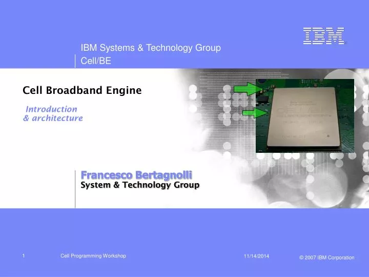
Cell Broadband EngineIntroduction& architecture Francesco Bertagnolli System & Technology Group Cell Programming Workshop
Agenda • Cell introduction • Cell architecture • SDK 3.0 • Linux on ps3 • Cell basic programming • Hands-on • Cell applications Cell Programming Workshop
Systems and Technology Group Cell History • IBM, SCEI/Sony, Toshiba Alliance formed in 2000 • Austin-based Design Center opened in March 2001 • Single CellBE operational Spring 2004 • February 7, 2005: First technical disclosures • November 9, 2005: Open source SDK & simulator published • February 8, 2006: IBM announced Cell Blade • July 2006: SDK 1.1 available • Sep 2006: GA of IBM Blade Center QS20 • Dec 2006: SDK 2.0 available • Oct 2007: SDK 3.0 available • Oct 2007: QS21 available • May 2008: QS22 available!! Cell Programming Workshop
1 TFlop Single Precision Floating Point (Mflops) 1 GFlop Year Introduction Cell Programming Workshop
Overview of the Cell Broadband Engine Processor The CBE processor is the first implementation of a new multiprocessor family conforming to the Cell Broadband Engine Architecture (CBEA) The CBEA and the CBE processor are the result of a collaboration between Sony, Toshiba, and IBM known as STI, formally begun in early 2001 Although the CBE processor is initially intended for applications in media-rich consumer-electronics devices such as game consoles and high-definition televisions, the architecture has been designed to enable fundamental advances in processor performance. The Cell Broadband Engine Architecture has been designed to support a very broad range of applications (commercial, scientific fields...) Cell Programming Workshop
Cell Competitive Roadmap Next Gen (2PPE’+32SPE’)45nm SOI ~1 TFlop (est.) Performance Enhancements/Scaling EnhancedCell BE(1+8eDP SPE)65nm SOI Cell BE(1+8)90nm SOI Cell BE(1+8)65nm SOI CostReduction All future dates and specifications are estimations only; Subject to change without notice. Dashed outlines indicate concept designs. Cell Programming Workshop
Committed Concept Cell Broadband Engine Architecture BladesIBM BladeCenter QS20 and beyond Target availability: 1H10 BladeCenter QS2Z • First CBEA teraflop processor • 2PPE’+32 eSPE • Power Architecture compliant • ~2 TFLOPS SP per blade • ~1 TFLOPS DP per blade • Next generation memory technology Target availability: 1H08 BladeCenter QS2Y • 2 CBEA-compliant processors • 1PPE + 8eDP SPE • SP: 460 GFLOPS per blade • eDP: 217 GFLOPS per blade • Up to 32 GB memory • PCI Express™ x16 slots Target availability: 4Q07 BladeCenter QS2X • 2 Cell/B.E. processors • 1PPE + 8SPE • SP: 460 GFLOPS per Cell blade • DP: 42 GFLOPS per Cell blade • Next Generation I/O chip • 2 GB memory SDK 5.0 GA September 2006 BladeCenter QS20 • 2 Cell/B.E. processors • 1PPE + 8SPE • SP: 460 GFLOPS per Cell blade • DP: 42 GFLOPS per Cell blade • 1 GB memory SDK 4.0 Target release: December 08 SDK 2.1 SDK 3.0 Target release: 08 SDK 1.1 Available:March 07 Target release:September 07 Available July 2006 2006 2007 2008 2009-2010 Cell Programming Workshop
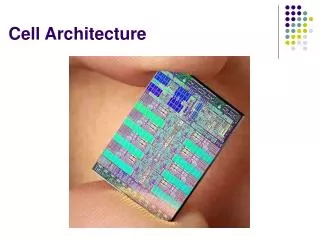
Cell Basic Design Concept Cell Programming Workshop
Where Have All the Transistors Gone …? • Cache • Deep Pipelining • Out-of-Order Processing X Add Performance … and Inefficiency X X Cell Programming Workshop
Cell Concept Three Major Limiters to Processor Performance • Power Wall • Hard limit to acceptable system power • Memory Wall • Processor frequency vs. DRAM memory latency • Frequency Wall • Increased efficiency and performance • Non Homogenous Coherent Chip Multiprocessor • Allows an attack on the “Frequency Wall” • DMA architecture attacks “Memory Wall” • Design, low operating voltage attacks “Power Wall” Cell Programming Workshop
Cell/B.E. - ½ the space & power vs traditional approaches Cell/B.E. 3.2 GHz 9 Cores, ~230 SP GFlops Example Dual Core 349mm2, 3.4 GHz @ 150W 2 Cores, ~54 SP GFlops Please note, that on any traditional processor, the show ratio of cores to cache illustrated here remains ~50% of area. Cell Programming Workshop
Why Cell ? (1) • Cell/BE: General Purpose… • Flexibility • Parallelism multi-levels • Stream processing • Double pipeline into SPEs • Static scheduling pipeline: no buffer • Storage hierarchy Cell Programming Workshop
Why Cell ? (2) • Simple hardware LS • SPEs indipendent & synergistic • cluster with 8 • Several systems: • game, HDTV, Blades, supercomputing, cluster computing, mainframes, etc.. • Structure is not fix • MFC, DMA • Registers 128x128 (4x32) Cell Programming Workshop
Why Cell ? (3) • Technology 90-65-45.. nm • State of art • Software development support • Low consumer • Flaws? NO, It’s RISC.. FLEXIBILITY Cell Programming Workshop
High Perf Computing SCE PS3(Cell/B.E. + GPU) Professional Business Consumer Cell/B.E. enables scalable, shared architecture with full consumer to professional potential IBM Roadrunner(16,000 Cell/B.E.s + AMD) IBM Cell/B.E. Blade(2 Cell/B.E.s)b Sony Cell/B.E. Computing Unit (Cell/B.E. + GPU + AV I/O) Mercury Cell/B.E. PCI Card(Cell/B.E. + Network) Common Operating Systems, Infrastructure, Tools, Libraries, Code… Cell Programming Workshop
Challenges of Digital Future – System integration and flexibility • Integration of offload engines and accelerators into processor • Simpler system structure • Integration of bridge functionality • More efficient I/O designs Cell Programming Workshop
Cell Hardware components & performance Cell Programming Workshop
Hardware Environment Block diagram of the CBE processor hardware • The Processor Elements • Memory Interface Controller • Element Interconnect Bus • Cell Broadband Engine Interface Unit Cell Programming Workshop
Synergistic Processor Elements Cell Broadband Engine Interface Unit Memory Interface Controller Element Interconnect Bus PowerPC Processor Element Cell Programming Workshop
EIB PPE L2 64-bit Power Architecture with VMX PPU L1 PXU • Power Processor Elements: PPE L2 PPU • The PowerPC Processor Element (PPE) features: • a general-purpose 64-bit RISC processor • conforms to the PowerPC Architecture • dual-threaded • with vector/SIMD multimedia extensions Cell Programming Workshop
PPE responsability: o responsible for overall control of a CBE system o run the operating systems • It has: • 32 KB level-1 (L1) instruction and data caches • 512 KB level-2 (L2) unified (instruction and data) cache The PPE supports the standard PowerPC Architecture instructions and the vector/SIMD multimedia extensions Cell Programming Workshop
PPE Registers 32 General-Purpose Registers (GPRs)—Fixed-point instructions operate on the full 64-bit width of the GPRs. 32 Floating-Point Registers (FPRs), 64 bits wide. The internal format of floating- point data is the IEEE 754 double-precision format. Single-precision results are maintained internally in the double-precision format. 64-bit LR - to hold the effective address of a branch target. 64-bit CTR - to hold either a loop counter or the effective address of a branch target. 64-bit XER - contains the carry and overflow bits and the byte count for the move-assist instructions. 32 128-bit-wide VMRs - served as source and destination registers for all vector instructions. Cell Programming Workshop
PPE multithreading The PPE hardware supports two simultaneous threads of execution To software, the PPE appears to provide two independent instruction-processing units. The threads appear to be independent because the PPE provides each thread with a copy of architectural state (registers), but the threads are not completely independent because many execution resources are shared by the threads to reduce the hardware cost of multithreading. To software, the PPE implementation of multithreading looks similar to a multiprocessor implementation, but there are several important differences It has duplicate sets of the PowerPC and vector user-state register files (one set for each thread) Cell Programming Workshop
PPE Multithreading vs Multi-Core Implementations Table compares the PPE multithreading implementation to a conventional dual-core microprocessor Cell Programming Workshop
PPE Block Diagram Pre-Decode L1 Instruction Cache L2 Interface Fetch Control Thread A Thread B Branch Scan SMT Dispatch (Queue) Microcode L1 Data Cache Decode Thread A Dependency Thread B Issue Thread A VMX/FPU Issue (Queue) Load/Store Unit Fixed-Point Unit Branch Execution Unit VMX Load/Store/ Permute VMX Arith./Logic Unit FPU Arith/Logic Unit FPU Load/Store Completion/Flush VMX Completion FPU Completion Cell Programming Workshop
SPU SPU SPU SPU SXU SXU SXU SXU LS LS LS LS SPE … MFC MFC MFC MFC EIB • Synergistic Processor Elements: SPEs SPE1 SPE SPU SPU Core (SXU) • Each SPE: • RISC core • 256 KB SRAM Local Store for instructions and data • 128X128-bit register file • support a special SIMD instruction set Channel Unit Local Store MFC(DMA Unit) • DMA Unit: Transfers data between Local Store and Main Memory To Element Interconnect Bus Cell Programming Workshop
Synergistic Processor Element (SPE) The eight identical SPEs are single-instruction, multiple-data (SIMD) processor elements are optimized for data-rich operations allocated to them by the PPE. • It is not optimized for running an operating system • The SPEs are independent processor elements, each running their own individual application programs or threads • The SPEs are designed to be programmed in high-level languages, such as C/C++ • They support a rich instruction set that includes extensive SIMD functionality • However, use of SIMD data types is preferred, not mandatory Cell Programming Workshop
SPU Organization Cell Programming Workshop
SPE Registers 128 of 128-bit General-Purpose Registers (GPRs) that can be used to store all data types The Floating-Point Status and Control Register (FPSCR) records information about the result and any associated exceptions. Cell Programming Workshop
One Difference between PPE and SPEs ... The more significant difference between the SPE and PPE lies in how they access memory The PPE accesses main storage with load and store instructions that move data between main storage and a private register file, the contents of which may be cached The SPEs, in contrast, access main storage with direct memory access (DMA) commands that move data and instructions between main storage and a private local memory, called a local store or local storage (LS). The LS has no associated cache This 3-level organization of storage (register file, LS, main storage) is a radical break from conventional architecture and programming models Cell Programming Workshop
512 kB L2-Cache CHIP CELL BE 16x16 kB Sub-Array 4x128 kB L2-Cache Sub-Array 32 kB L1 Data-Cache 32 kB L1 Instruction-Cache 256 kB Local Store • System Memory Cell Programming Workshop
EIB MIC Dual XDRTM • Memory Interface • 16 B/cycle • 25.6 GB/s (@1.6 Ghz) • Memory Interface Controller - MIC The MIC provides the interface between the EIB and physical memory It supports one or two Rambus extreme data rate (XDR) memory interfaces (which together support between 64 MB and 64 GB of XDR DRAM memory) XDR Dram is ECC-protected, with multi-bit error detection and optional single bit error correction Cell Programming Workshop
EIB BEI FlexIOTM • Element Interconnect Bus - EIB • Cell Broadband Engine Interface Unit – (BEI) • On chip coherent bus • 96B / cycle bandwidth • 2 Rings in each direction BEI • I/O Interface • Can be coherent • 16 B/cycle x 2 EIB Cell Programming Workshop
Cell performance Cell Programming Workshop
>100 GFLOPs DP in 65nm Cell is not a collection of different processors, but a synergistic whole Cell Programming Workshop
>100 GFLOPs DP in 65nm Cell Programming Workshop
Source: Cell Broadband Engine Architecture and its first implementation – A performance view, http://www-128.ibm.com/developerworks/library/pa-cellperf/ Cell Programming Workshop
Key Performance Characteristics • Cell's performance is about an order of magnitude better than GPP for media and other applications that can take advantage of its SIMD capability • Performance of its simple PPE is comparable to a traditional GPP performance • its each SPE is able to perform mostly the same as, or better than, a GPP with SIMD running at the same frequency • key performance advantage comes from its 8 de-coupled SPE SIMD engines with dedicated resources including large register files and DMA channels • Cell can cover a wide range of application space with its capabilities in • floating point operations • integer operations • data streaming / throughput support • real-time support Cell Programming Workshop
Cell Blade Cell Programming Workshop
XDRAM XDRAM Cell Processor Cell Processor South Bridge South Bridge GbE GbE IB 4X IB 4X BladeCenter Network Interface The First Generation Cell Blade 1GB XDR Memory Cell Processors IBM Blade Center interface Cell Programming Workshop
- 2 Cell Chips pro QS21-Blade - 14 QS21 Blades pro BladeCenter • 60 Watt pro Cell BladeCenter-H 14 blades • Peak Performance • Up to 460 GFLOPS per blade • Up to 6.4 TFLOPS in a single BladeCenter H chassis • Up to 25.8 TFLOPS in a standard 42U rack Cell Programming Workshop
IBM BladeCenter IBM BladeCenter Thinkpad T60 Thinkpad T60 Thinkpad T60 echo Thinkpad Thinkpad C:\IBM\product\Cell\_ echo Thinkpad Thinkpad C:\IBM\product\Cell\_ echo Thinkpad Thinkpad C:\IBM\product\Cell\_ echo Thinkpad Thinkpad C:\IBM\product\Cell\_ echo Thinkpad Thinkpad C:\IBM\product\Cell\_ echo Thinkpad Thinkpad C:\IBM\product\Cell\_ IBM QS21 IBM QS20 IBM QS20 IBM QS20 IBM QS20 IBM QS20 IBM QS20 IBM QS20 IBM QS20 Eth. Switch IB <> Eth. InfiniBand InfiniBand • Workstations Server architecture echo Thinkpad Thinkpad C:\IBM\product\Cell\_ echo PC PC C:\IBM\product\Cell\_ echo Thinkpad Thinkpad C:\IBM\product\Cell\_ echo PC PC C:\IBM\product\Cell\_ back Cell Programming Workshop
IBM BladeCenter QS21 • Announcement: August 28, 2007 Cell Programming Workshop
IBM BladeCenter QS22 Cell Programming Workshop
IBM BladeCenter QS22: specifications Cell Programming Workshop
Where to get more Cell BE information? Cell Programming Workshop
Cell Resource • Cell resource center at developerWorks • http://www-128.ibm.com/developerworks/power/cell/ • Cell developer's corner at power.org • http://www.power.org/resources/devcorner/cellcorner/ • The cell project at IBM Research • http://www.research.ibm.com/cell/ • The Cell BE at IBM alphaWorks • http://www.alphaworks.ibm.com/topics/cell • Cell BE at IBM Engineering & Technical Services • http://www-03.ibm.com/technology/ • IBM Power Architecture • http://www-03.ibm.com/chips/power/ • Cell BE documentation at IBM Microelectronics • http://www-306.ibm.com/chips/techlib/techlib.nsf/products/Cell_Broadband_EngineCell • Linux info at the Barcelona Supercomputing Center website • http://www.bsc.es/projects/deepcomputing/linuxoncell/ Cell Programming Workshop
Cell Education • Online courses at IBM Education Assistant • http://publib.boulder.ibm.com/infocenter/ieduasst/stgv1r0/index.jsp • Online courses at IBM Learning • http://ibmlearning.ibm.com/index.html • Podcasts at power.org • http://www.power.org • Onsite classes at IBM Innovation Center • https://www-304.ibm.com/jct09002c/isv/spc/events/cbea.html Cell Programming Workshop
Cell BE Documentation • The following documents define the Cell Broadband Engine architecture, programming using the SDK, the new IBM BladeCenter QS20, XL C/C++compiler, Full-System Simulator, and the PowerPC base architecture. • Cell Broadband Engine • Cell Broadband Engine Architecture V1.01 (updated) • Cell Broadband Engine Programming Handbook V1.0 • Cell Broadband Engine Registers V1.4 (updated) • SPU C/C++ Language Extensions V2.2.1 (updated) • Synergistic Processor Unit (SPU) Instruction Set Architecture V1.11 (updated) • SPU Application Binary Interface Specification V1.5.1 (updated) • SPU Assembly Language Specification V1.4 (updated) Cell Programming Workshop
Cell BE Documentation • Cell Broadband Engine Programming using the SDK • Cell Broadband Engine SDK Installation Guide V2.0 (updated) • Cell Broadband Engine SDK Programmer's Guide V1.0 (new) • Cell Broadband Engine Programming Tutorial V2.0 (updated) • Cell Broadband Engine Linux Reference Implementation Application Binary Interface Specification V1.1 (updated) • SPE Runtime Management library documentation V1.2 (updated) • SPE Runtime Management library documentation V2.0 (new) • Cell Broadband Engine SIMD Math Library Specification V1.0 (new) • Accelerator Library Framework Programming Guide and API Reference V1.0 (new) • Sample Library documentation V2.0 (updated) • IDL Compiler for Remote Procedure Calls • Post-link Optimization Utility (new) Cell Programming Workshop