Download
1 / 10
120 likes | 191 Vues
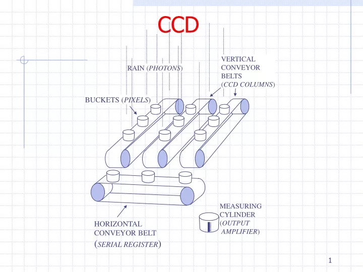
CCD. VERTICAL CONVEYOR BELTS ( CCD COLUMNS ). RAIN ( PHOTONS ). BUCKETS ( PIXELS ). MEASURING CYLINDER ( OUTPUT AMPLIFIER ). HORIZONTAL CONVEYOR BELT ( SERIAL REGISTER ). 15 m m. CCD. All astronomical CCD’s are thin, backside illuminated

E N D
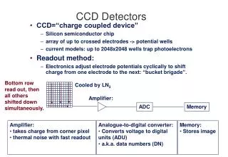
CCD VERTICAL CONVEYOR BELTS (CCD COLUMNS) RAIN (PHOTONS) BUCKETS (PIXELS) MEASURING CYLINDER (OUTPUT AMPLIFIER) HORIZONTAL CONVEYOR BELT (SERIAL REGISTER)
15mm CCD • All astronomical CCD’s are thin, backside illuminated • Consumer CCD’s are thick, frontside illuminated Anti-reflective (AR) coating Incoming photons p-type silicon n-type silicon Polysilicon electrodes Incoming photons p-type silicon n-type silicon Silicon dioxide insulating layer 625mm Polysilicon electrodes
CCD 160mm Photomicrograph of a corner of an EEV CCD. Image Area Serial Register Bus wires Edge of Silicon Read Out Amplifier The serial register is bent double to move the output amplifier away from the edge of the chip. This useful if the CCD is to be used as part of a mosaic.The arrows indicate how charge is transferred through the device.
1 2 1 2 1 2 1 2 3 3 3 3 CCD
CCD Image area Metal,ceramic or plastic package Connection pins Gold bond wires Bond pads Silicon chip On-chip amplifier Serial register
CCD The diagram shows a small section (a few pixels) of the image area of a CCD. This pattern is reapeated. Channel stops to define the columns of the image Plan View Transparent horizontal electrodes to define the pixels vertically. Also used to transfer the charge during readout One pixel Electrode Insulating oxide n-type silicon p-type silicon Cross section Every third electrode is connected together. Bus wires running down the edge of the chip make the connection. The channel stops are formed from high concentrations of Boron in the silicon.
CCD Camera Thermally Electrical feed-through Vacuum Space Pressure vessel Pump Port Insulating Pillars Face-plate . . Telescope beam Boil-off . Optical window CCD CCD Mounting Block Thermal coupling Nitrogen can Activated charcoal ‘Getter’ Focal Plane of Telescope
CCD Camera Retaining clamp Temperature servo circuit board CCD Aluminised Mylar sheet Gold plated copper mounting block Top of LN2 can Platinum resistance thermometer Pressure Vessel ‘Spider’. The CCD mounting block is stood off from the spider using insulating pillars. Location points (x3) for insulating pillars that reference the CCD to the camera face-plate Signal wires to CCD
CCD • Buried channel MOS type p-n type