Download
1 / 12
120 likes | 415 Vues
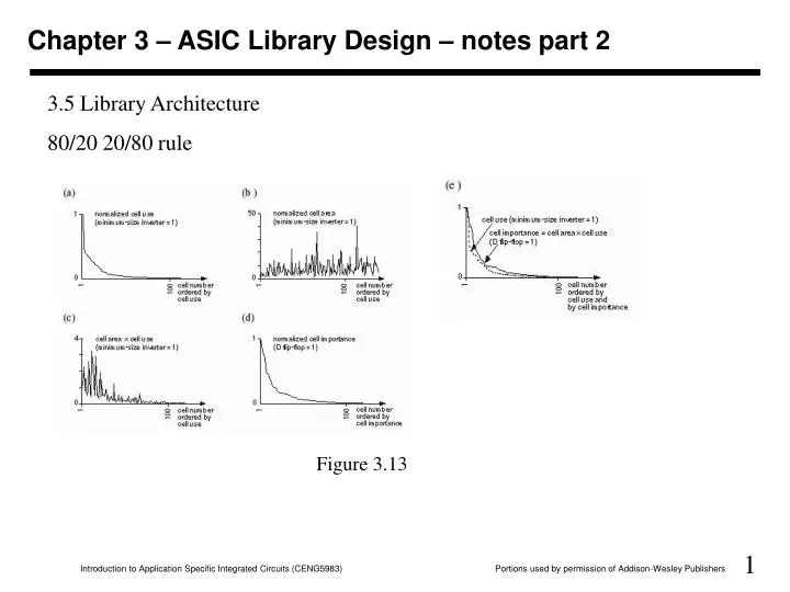
Chapter 3 – ASIC Library Design – notes part 2. 3.5 Library Architecture 80/20 20/80 rule. Figure 3.13. 3.6 Gate Array Design. Gate-array base cell (or base cell) Gate-array base (or base or base array) Gate-isolated gate array – an off gate (transistor) is used to isolate active gates

E N D
Chapter 3 – ASIC Library Design – notes part 2 3.5 Library Architecture 80/20 20/80 rule Figure 3.13
3.6 Gate Array Design • Gate-array base cell (or base cell) • Gate-array base (or base or base array) • Gate-isolated gate array – an off gate (transistor) is used to isolate active gates • Oxide isolation – field oxide is used to isolate gates (in individual tubs) • Horizontal tracks – horizontal tracks (channels) for routing (m1) • Vertical tracks – vertical tracks (channels) for routing (m2)
3.6 Gate Array Design (cont) Figure 3.14 – Gate-isolated gate-array
3.6 Gate Array Design (cont) Figure 3.15 – Oxide-isolated gate-array
3.6 Gate Array Design (cont) Figure 3.16 – Oxide-isolated gate-array
3.6 Gate Array Design (cont) Figure 3.17 – Flip-flop macro in a gate-isolated gate-array
3.6 Gate Array Design (cont) Figure 3.18 – SiARC/Synopsys cell-based array (CBA) basic cell
3.7 Standard Cell Design Fig. 3.19 standard cell from Fig. 1.3
3.7 Standard Cell Design (cont) Fig. 3.20 – A D flip-flop standard cell • Layout using 45 deg angles • Transistor sizes vary to optimize area and performance • Power rails are at the top and bottom • M1 for power rails and local interconnect, M2 for cell connections
3.8 Datapath-Cell Design Fig 3.21 – Datapath D flip-flop
3.8 Datapath-Cell Design (cont) Fig. 3.22 – Schematic for D FF shown in Fig. 3.21
3.8 Datapath-Cell Design (cont) Datapath design using 2 metal layers and routing channels Datapath design using 3 metal layers and routing over the cells