Download
1 / 29
300 likes | 493 Vues
“ More-than-Moore ” ERD. Michel Brillouët – U-In Chung + other coming contributions. rf wave. 011001010…. control. “ More-than-Moore ” ERD: technical background. Example: Wireless Sensor Networks. Higher level function. ADC. LNA. Intermediate level function. nanoradio. LO. PA. DAC.

E N D
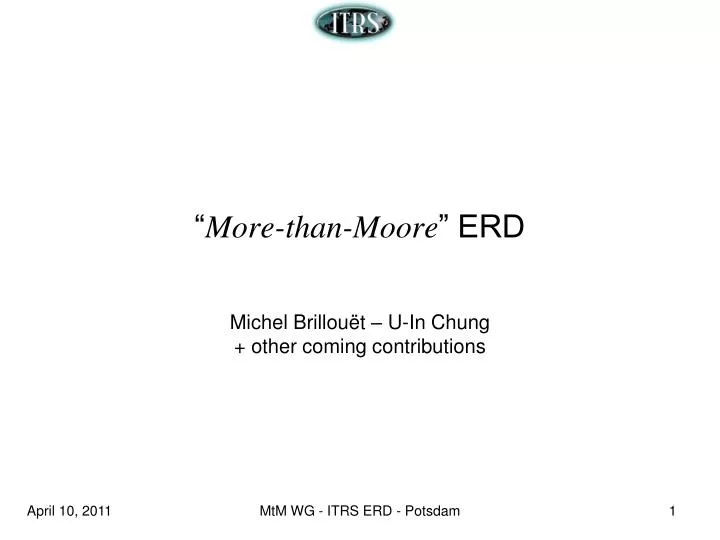
“More-than-Moore” ERD Michel Brillouët – U-In Chung+ other coming contributions MtM WG - ITRS ERD - Potsdam
rf wave 011001010… control “More-than-Moore” ERD: technical background Example: Wireless Sensor Networks Higher level function ADC LNA Intermediate levelfunction nanoradio LO PA DAC switch? antenna filter oscillator mixer converter LO Lower level functions ADC nanoantenna spin-torque oscillator RTD? Energy C-electronics NEMS nanoresonator SET? MtM WG - ITRS ERD - Potsdam 2011 ITRS-ERD MtM devices
“More-than-Moore” ERD: structure of the contributions • identify key figures of merit for the device / function (see general MtM methodology from the ITRS White Paper) • if available give figures for the state-of-the-art “classical” devices and their predicted value “at the end of the roadmap” (if possible refer to existing tables in the other ITRS chapters) • list potential emerging devices and give figures for demonstrated and extrapolated performances along the same metrics • list a first set of significant publications supporting this exercise • add any qualitative statement as needed MtM WG - ITRS ERD - Potsdam
“More-than-Moore” ERD: working group rationales, technical content, method, etc. M. Brillouët introduction spin-torque oscillator A. Chen U-In Chung as rf transistor, mixer… C-electronics S. Das or any other non-linear emerging device rectifier A. Ionescu NEMS nanoresonator M. Brillouët (p.i.) assess if there is significant activity RTD? only if someone volunteers SET? Other volunteers: H. Bennett, S. Deleonibus, Y. Obeng [+ G. Bourianoff, E. De Benedictis, S. Shankar??] MtM WG - ITRS ERD - Potsdam
Figures of merit for rf ERD M. Brillouët MtM WG - ITRS ERD - Potsdam
rf-ams transistors rf-ams CMOS rf-ams bipolar • gm/gds • matching • noise (1/f, NF) • ft, fMax@ some BV MtM WG - ITRS ERD - Potsdam from ITRS Wireless chapter
Transistors for power amplifier III-V HBT Si MOS SiGe HBT • fMax • linear efficiency@ some BV MtM WG - ITRS ERD - Potsdam from ITRS Wireless chapter
Base station devices etc. MtM WG - ITRS ERD - Potsdam
Conclusion • device FoM useful for comparing with graphene / C-based rf transistors • FoM and state-of-the-art / “end of the roadmap” have to be defined for: • oscillators • switch • ADC MtM WG - ITRS ERD - Potsdam
Graphene / C-based electronicsfor rf applications U-In Chung + M. Brillouët MtM WG - ITRS ERD - Potsdam
Graphene RF Transistors Key figures of merit of Graphene RF Transistor • Possibility of THz cutoff frequency • - Sub-100-nm transistors were fabricated using nanowire gate. • High Fermi velocity of carriers in graphene, resulting in high drift velocity (~ 4 x 107 cm/s) in channel, makes fT ~ 1THz for sub 70 nm channel length device
Comparison to Current Devices Highest cutoff frequency of Current Devices UCLA [1] • GaAs mHEMT with a 20-nm gate: 660 GHz • Si MOSFET with a 29-nm gate: 485 GHz. • GaAs pHEMT with a 100-nm gate: 152 GHz. SAMSUNG [3] IBM (Science) Left: RF Transistors on 6 inch wafer Right: Single RF Transistor F.Schwierz, “Graphene Transistors,” Nature Nanotechnology 5, 487 (2010)
Potential applications Needs and Destination of next generation mobile • Low Noise Amplifier • Mixer
Challenges Defect-free monolayer graphene growth Graphene-dielectric, graphene-metal inferface : CVD graphene has satisfactory uniformity of thickness[7]but transfer process, which is prerequisite for CVD graphene, generate tearing of graphene. : epitaxial one has no need for transfer, therefore no issue of transfer process, but unsatisfactory uniformity of thickness[5]. : Graphene is highly inert material, which reduces the adhesion between graphene and dielectric or metal. : Charge impurities on the SiO2 surface reduces mobility of graphene. : Hexagonal boron nitride is known as best surface for graphene, however, the low temperature growth method would need to be developed.
References [1]L. Liao, Y.-C. Lin, M.Bao, R. Cheng, J.Bai, Y. Liu, Y.Qu, K. L. Wang, Y. HuangX.Duan, “High-speed graphene transistors with a self-aligned nanowire gate,” Nature 467, 305 (2010) [2]Ph. Avouris, Y.-M. Lin, F. Xia, D.B. Farmer, T. Mueller, C. Dimitrakopoulos, K. Jenkins, A. Grill, “Graphene-Based Fast Electronics and Optoelectronics,” IEDM 23.1 (2010) [3]J. Lee, H.-J. Chung, J. Lee, H. Shin, J. Heo, H. Yang, S.-H. Lee, J. Shin, S. Seo, U. Chung, I. Yoo, K. Kim, “RF Performance of Pre-Patterned Locally-Embedded-Back-Gate Graphene Device,” IEMD 23.5 (2010) [4]X. Li, W.Cai, J. An, S. Kim, J. Nah, D. Yang, R.Piner, A.Velamakanni, I. Jung, E.Tutuc, S. K. Banerjee, L. Colombo, R. S. Ruoff,“Large-Area Synthesis of High-Quality and Uniform Graphene Films on Copper Foils,” Science 324, 1312 (2009) [5] C. Berger, Z. Song, T. Li, X. Li, A. Y. Ogbazghi, R.Feng, Z. Dai, A. N. Marchenkov, E. H. Conrad, P. N. First, W. A. de Heer, “Ultrathin Epitaxial Graphite: 2D Electron Gas Properties and a Route toward Graphene-based Nanoelectronics,” J. Phys. Chem. B 108, 19912 (2004) [6]J.S.Moon, D. Curtis, S. Bui, T. Marshall, D. Wheeler, I. Valles, S. Kim, E. Wang, X. Weng, M. Fanton,“Top-Gated Graphene Field-Effect Transistors Using Graphene on Si (111) Wafers,”IEEE Elect. Dev. Lett. 31, 1193 (2010) [7]I.Jeon, H. Yang, S.-H.Lee, J.Heo, D. H. Seo, J. Shin, U-I.Chung, Z. G. Kim, H.-J. Chung, S.Seo, “Passivation of Metal Surface States: Microscopic Origin for Uniform Monolayer Graphene by Low Temperature Chemical Vapor Deposition,” ACS Nano 5, 1915 (2011) [8]D.Waldmann, J.Jobst,F. Speck,T.Seyller, M. Krieger, H. B. Weber, “Bottom-gated epitaxial graphene,” Nature Materials online edition (2011) [9]L. Liao, J.Bai, R. Cheng, Y.-C. Lin, S. Jiang, Y.Qu, Y. Huang, X.Duan, “Sub-100 nm Channel Length Graphene Transistors,” Nano Lett. 10, 3952 (2010) [10] F.Schwierz, “Graphene Transistors,” Nature Nanotechnology 5, 487 (2010)
Latest results on ft / fMax ↘ parasitics (R, C…) • gm/gds • matching • noise (1/f, NF) • ft, fMax@ some BV ↗ µ or v from F. Schwierz Nature 472 41 (2011) MtM WG - ITRS ERD - Potsdam
gate ox. Al + ALD Al2O3 Au/Pd contacts grapheneCVD on Cu transfer w. PMMA 134meV surface phonon low Dit DLC SiO2 59meV surface phonon high Dit rf CVD graphene transistors • from static Id-Vd • Dirac point -7V ⇐ fixed charge • short channel effect (low Vg modulation of Id) ft = 155GHz @Lg=40nm from rf measurementswith de-embedding no T dependency fMax=20GHz @ Lg=550nm fMax=13GHz @ Lg=140nm Rc limited? MtM WG - ITRS ERD - Potsdam from Y. Wu Nature 472 74 (2011)
Graphene for rf mixer full-wave rectifier → frequency doubling frequency mixer if... → no odd-order inter-modulation T. Palacios et al. IEEE Comm. Mag. 48 122 (2010) MtM WG - ITRS ERD - Potsdam
Graphene for rf NEMS resonator rf switch • high stiffness • low density potential GHz high current capability (>7 kA/cm²) Actual: Q = 104 @5K 50-80 MHz high Rc K.M. Milaninia et al. APL 95 183105 (2009) C. Chen et al. Nature Nano 4 861 (2009) MtM WG - ITRS ERD - Potsdam
Spin-Torque nano-oscillators U-In Chung MtM WG - ITRS ERD - Potsdam
Spin torque oscillator Key figures of merit of spin torque oscillator 1. frequency tunability ( 0.1 GHz ~ 40GHz or more) - frequency can be tuned by external magnetic field or spin torque current - frequency can also be tuned by magnetic materials and structures 2. compact size (nanometer-sized oscillator) - cost effective STO size : ~ 100 ⅹ 100 nm2
Potential applications Needs and Destination of next generation mobile • Mobile convergence • Reconfigurability • Low power • Compact Design STO : Wideband tunable nano-oscillator
Challenges Auto-oscillation structures Increase of Output Power Phase noise (phase stability) : Spin torque oscillators have to eliminate the need for external magnetic field that is used for most current experimental demonstrations. : Now, three different approaches have been suggested for the auto-oscillation. (perpendicular polarizer + in-plane free layer, wavy spin torque, magnetic vortex structures) : The best metallic spin-transfer oscillators (MTJ oscillators) measured to date produce about 100 pW(~140 nW), while a few microwatts would likely be required for practical GHz communication applications : For the increase of output power, synchronization of spin torque oscillators has been proposed. If phase locking is achieved for a collection of N oscillators, depending on how the devices are wired, the maximum output power may grow as quickly as N2. : For the most of telecommunication applications, low phase noise is extremely important issues. The nonlinearities of spin torque oscillators are main sources of frequency instabilities, which result in the broadening of linewidth of oscillation spectrum. : Synchronization of spin torque oscillators is also one of the possible solutions.
References Experimental Demonstrations [2003] Nature_425_380_Microwave oscillation of nanomagnet driven by a spin-polarized current [2004] Phys.Rev.Lett._92_027201_Direct current induced dynamics in CoFe NiFe point contacts [2005] Nature_437_389_Mutual phase-locking of microwave spin torque nano-oscillators [2005] Nature_437_393_Phase-locking in double point contact spin tranfer devices [2008] Nat.Phys._04_803_Bais driven high power microwave emission from MgO based TMR devices Auto-oscillation structures [2007] Nat.Mat._06_447_Spin-torque oscillator using a perpendicular polarizer and a planar free layer [2007] Nat.Phys._03_498_Magnetic vortex oscillator driven by d.c. spin-polarized current [2007] Nat.Phys._03_492_Shaped angular dependence of the spin-transfer torque and microwave generation without magnetic field Issues of Challenges(phase noise) [2008] Phys.Rev.Lett._100_017207_Generation Linewidth of an Auto-Oscillator with a Nonlinear Frequency shift Spin-Torque Nano-Oscillator [2009] Phys.Rev.Lett._102_257202_Temporal Coherence of MgO Based Magnetic Tunnel Junction Spin Torque Oscillators
NEMS resonators A. Ionescu to be provided later MtM WG - ITRS ERD - Potsdam
RTD for ADC M. Brillouët MtM WG - ITRS ERD - Potsdam
RTD for ADC • from the Web of Science (RTD AND ADC): • only 6 papers from 1993 to 2011 (+2 from the references) • Benefits • lower device count → low power consumption • high speed (sub-ps switching time) • Issues • use of III-V (InGaAs) [issue from the past?] • low peak-to-valley current ratio • variability • Proposal • drop RTD for ADC as a specific topic • extend a later survey into NDC-devices for ADC? MtM WG - ITRS ERD - Potsdam
Back-up slides MtM WG - ITRS ERD - Potsdam