Download
1 / 22
570 likes | 2.8k Vues
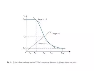
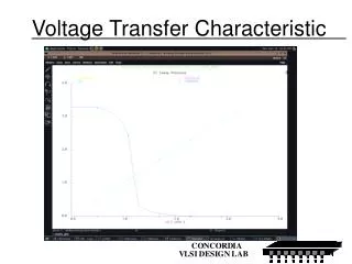
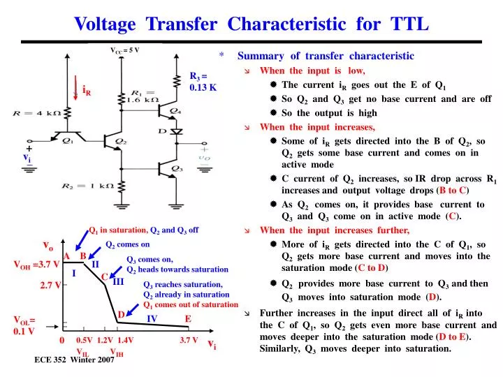
Voltage Transfer Characteristic for TTL. Summary of transfer characteristic When the input is low, The current i R goes out the E of Q 1 So Q 2 and Q 3 get no base current and are off So the output is high When the input increases,

E N D
Voltage Transfer Characteristic for TTL • Summary of transfer characteristic • When the input is low, • The current iR goes out the E of Q1 • So Q2 and Q3 get no base current and are off • So the output is high • When the input increases, • Some of iR gets directed into the B of Q2, so Q2 gets some base current and comes on in active mode • C current of Q2 increases, so IR drop across R1 increases and output voltage drops (B to C) • As Q2 comes on, it provides base current to Q3 and Q3 come on in active mode (C). • When the input increases further, • More of iR gets directed into the C of Q1, so Q2 gets more base current and moves into the saturation mode (C to D) • Q2 provides more base current to Q3and thenQ3moves into saturation mode (D). • Further increases in the input direct all of iRintothe C of Q1, so Q2 gets even more base current and moves deeper into the saturation mode (D to E). Similarly, Q3 moves deeper into saturation. VCC = 5 V R3 = 0.13 K iR + vi _ Q1 in saturation, Q2 and Q3 off vo Q2 comes on A B Q3 comes on, Q2 heads towards saturation VOH =3.7 V II I C III 2.7 V Q3 reaches saturation, Q2 already in saturation Q1 comes out of saturation D IV E VOL= 0.1 V 0 vi 0.5V 1.2V 1.4V 3.7 V VIL VIH Bipolar Digital Pt. 4
Voltage Transfer Characteristic for TTL • Noise Margins • Noise Margin for low state NML = VIL -VOL • VOL = low output voltage for typical high input voltage = 0.1 V • VIL= maximum input voltage recognized as a low input = 0.5 V • NML = VIL-VOL =0.5 V - 0.1 V = 0.4 V • Noise Margin for high state NMH = VOH -VIH • VOH = high output voltage for typical low input voltage = 3.7 V • VIH= minimum input voltage recognized as a high input = 1.4 V • NMH = VOH -VIH = 3.7 V- 1.4V = 2.3 V • Noise margins are very unequal for this technology. VCC = 5 V iR + vi vo _ vo A B VOH =3.7 V II I C IV III 2.7 V NMH NML D E VOL= 0.1 V 0 vi 0.5V 1.2V 1.4V 3.7 V VIL VIH Bipolar Digital Pt. 4
Comparison of Simplified TTL and TTL VCC = 5V VCC = 5V RC = 1.6K R=4K + vo • Noise Margin (Low state) • NML = VOL - VIL = 0.6V - 0.1 V = 0.5 V • Noise Margin (High state) • NMH = VOH - VIH = 5 V - 0.7 V = 4.3 V • Noise Margin (Low state) • NML = VOL - VIL = 0.5V - 0.1 V = 0.4 V • Noise Margin (High state) • NMH = VOH - VIH = 3.7 V – 1.4 V = 2.3 V vo vo A B A B 3.7 V II VCC = 5V I C IV III I II III 2.7 V NML C NMH D D NMH 0.2V 0.1V NML E VOL= 0.1 V vi 0 vi 0.5V 1.2V 1.4V 3.7 V VIL VIH 0.6 V 0.7V 5 V VOL= 0.1 V Bipolar Digital Pt. 4
Voltage Transfer Characteristic for TTL • What is the function of Q4? • Q4 is weakly on but producing little current when the output is low. • This helps to minimize power dissipation since Q3 is on and in saturation so ready to conduct current. • Q4 is weakly on when the output is high. • This is because the following gate has a reverse biased E junction for Q1 and so draws almost no current. • The reason Q4 is included in the circuit is to provide a large current to ensure a fast transition time when the output is going from low to high so tPLH is small. • At all other times we want Q4 off (or only weakly on) to minimize power dissipation. • A simple resistor in place of Q4 gives a very long rise time ~ 100’s nsec, as we saw for the RTL inverter, so the use of Q4 and the diode D is an improvement. VCC = 5 V iR + vi vo _ vo A B VOH =3.7 V II I C III 2.7 V D IV E VOL= 0.1 V 0 vi 0.5V 1.2V 1.4V 3.7 V VIL VIH Bipolar Digital Pt. 4
Transistor - Transistor Logic (TTL) Fan – Out Capability • What is the ability (fan-out) of the TTL logic to drive simultaneously a number of subsequent inverters? • Fan-out = NMax = maximum number of subsequent inverters that can be simultaneously driven (connected to the output). • For the output high, i.e. vo = 3.7 V, the output is connected to a reverse biased E junction for Q1 for each subsequent inverter, so current load is very small. • However, for output low, i.e. vo = 0.1 V • E junction of each Q1 forward biased, so • So this adds to the collector current of Q3 so iC3 = N iE1 = N (1.0 mA) • Fan-out limit = maximum value of N • In saturation, iC3 < βiB3 • In active, iC3 = βiB3 • So limit is when Q3 comes out of saturation into active mode and iC3 = βiB3. VCC = 5 V R3 = 0.13 K iRi = 1 mA p n iC3 iE1 =1 mA + + VCE3 + _ vo _ sat Recall, we found when the output was low Fan-out limt Bipolar Digital Pt. 4
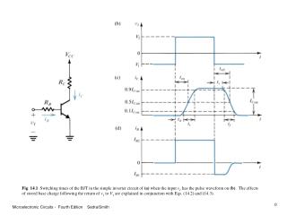
TTL Propagation Delay Output going high vo • Output going high • Input goes low • Transistors Q2 and Q3 turn off (cutoff) due to low input to gate. • Large charging current flows through Q4 to charge up C. • Q4 called pull-up transistor • Charging time is small ~ 1 nsec • tPLH is the time it takes the output to rise from VOL = VCE,sat = 0.1 V to 1/2(VOH + VOL) = ½(3.7+0.1) V = 1.9 V iC4 VOH= 3.7V iB4 iR Goes on 1.9V iE4 iCap Goes off Goes low + vo Goes high VCE,sat = 0.1 V C t Goes off tPLH Bipolar Digital Pt. 4
TTL Propagation Delay Output going high • Charging current for capacitor is emitter current of Q4. • At outset, vo= VCE,sat = 0.1 V, so iB4 and VCE4 are initially large • Charging current iCap≈ iE4 is large since for = 10 • As vo rises, iB4 decreases, so iE4 = iCap decreases, but Q4 stays in active mode. • At vo = 1.9V • So iE4 = iC hasdecreased to • So capacitor charging current is not constant and calculation of tPLH is more difficult. vo iC4 iB4 VOH= 3.7V 1.9V iE4 iCap VOH= 0.1V t tPLH vo C iC4 Goes high R S P vCE4 Bipolar Digital Pt. 4
TTL Propagation Delay Output going high • Approximating the charging current for capacitor as a constant (average value), • We can calculate the propagation delay tPLH using vo iC4 iB4 VOH= 3.7V iE4 iCap VOH= 0.2V t vo tPLH C iC4 Goes high R S So Q4 provides a large charging current to reduce the rise time for the output going high. P vCE4 Bipolar Digital Pt. 4
TTL Propagation Delay Output going low • Output going low • Input goes high • Transistors Q2 and Q3 turn on (first in active then saturation) as iR is redirected from the input into the base of Q2 • Q4 is turned off as VB4 = VCC – iR1 R1 decreases since iR1≈ iC2. • Large discharge current flows through Q3 • Q3 called pull-down transistor • Discharge time is small ~ 1 nsec • tPHL is time it takes the output to fall from VOH = 3.7 V to 1/2(VOH + VOL) = ½(3.7+0.1) V = 1.9 V vo iR1 VOH = 3.7V iR Goes off iB2 iCap 1.9V Goes on + iB3 vo Goes low iC3 Goes high VCE,sat = 0.1 V C t tPHL Goes on Bipolar Digital Pt. 4
TTL Propagation Delay Output going low VCC=5V vo iR VOH = 3.7V off 1.9V iE4=0 iB2 iCap on VCE,sat = 0.1 V + Goes high t iC3 tPHL vo on iB3 iC3 S R What current to use for the transistor? P vCE3 Bipolar Digital Pt. 4
Power Dissipation for Transistor - Transistor Logic (TTL) • For input high and output low. • Q2 and Q3are in SATURATION. • Since Q2 is in saturation mode, iC2<βiB2 but VCE2 = 0.2 V and • Q4 is weakly on, iC4 ≈ 0. • Power dissipation VCC = 5 V iR1 iC4=0 R3 = 0.13 K iR VB1 VC2 p io n + sat vi = 3.7V low _ sat Bipolar Digital Pt. 4
Power Dissipation for Transistor - Transistor Logic (TTL) • For input low and output high. • Q2 and Q3are off, iC2 ≈ 0,iC3 ≈ 0. • Q4 is weakly on, iC4 ≈ 0. • iR1 ≈ 0. • Q1 is on so VBE1 = 0.7 V • Power dissipation • Average Power Dissipation • Power Delay Product VCC = 5 V iR1=0 iC4=0 R3 = 0.13 K iR VB1 p io≈0 n + off Low =0.2V high _ off Bipolar Digital Pt. 4
TTL vs. Simplified TTL * Logic levels and noise margins • Noise Margin for Low State • NML = VIL – VO = 0.6 V - 0.1 V = 0.5V • Noise Margin for High State • NMH = VOH - VIH = 5 V - 0.7 V = 4.3 V • Unequal noise margins for high and low states. • Propagation delays • Output going low • Output going high • Propagation delay • Power – Delay Product vo vo vi vi * Logic levels and noise margins • Noise Margin for Low State • NML = VIL – VO = 0.5 V - 0.1 V = 0.4 V • Noise Margin for High State • NMH = VOH - VIH = 3.7 V – 1.4 V = 2.3 V • Unequal noise margins for high and low states. • Propagation delays • Output going low • Output going high • Propagation delay • Power – Delay Product Bipolar Digital Pt. 4
TTL Summary • Advantages: • Fast switching times, ~ 1 nsec. • Low power-delay product (~ 10 pJ) • Good fan-out capability • Adequate noise margins • Disadvantages: • Static power dissipation, higher than CMOS • Complexity – four transistors • Time delay due to saturating transistors. • Small noise margin for low state, e.g. 0.4 V. Bipolar Digital Pt. 4
Comparison of Digital Logic Families • J. Millman and A. Grabel, Microelectronics, McGraw Hill, p. 261 (1987). vo vi Bipolar Digital Pt. 4
TTL Gates Bipolar Digital Pt. 4
Schottky TTL Gates • Schottky diode clamp prevents transistors from going deep into saturation. • Reduces transistor switching time. • Reduces propagation delay, e.g. from ~ few nsec to < 1 nsec. • Power-delay product is not reduced due to lower resistances used. • Low power version of Schottky TTL has DP ~ 4 pJ. Bipolar Digital Pt. 4
Comparison of Digital Logic Families Power delay product = a constant Bipolar Digital Pt. 4
Comparison of Digital Logic Families Bipolar Digital Pt. 4
Emitter-Coupled Logic (ECL) • Sub nsec propagation delay (fastest of bipolar technologies). • 40 mW/gate power dissipation (high). • Power delay product = 30 pJ. • Noise margins nearly equal, ~ 0.15 V • High fan-out capability. Bipolar Digital Pt. 4
BiCMOS Basic Inverter Advanced Inverter Two input NAND Gate Bipolar Digital Pt. 4
Comparison of Digital Logic Families Bipolar Digital Pt. 4