Download
1 / 18
180 likes | 257 Vues
COMP541 Transistors and all that… a brief overview. Montek Singh Sep 8, 2014. Transistors as switches. At an abstract level, transistors are merely switches 3-ported voltage-controlled switch n-type: conduct when control input is 1 p-type: conduct when control input is 0.

E N D
COMP541Transistors and all that…a brief overview Montek Singh Sep 8, 2014
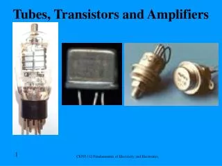
Transistors as switches • At an abstract level, transistors are merely switches • 3-ported voltage-controlled switch • n-type: conduct when control input is 1 • p-type: conduct when control input is 0
Silicon as a semiconductor • Transistors are built from silicon • Pure Si itself does not conduct well • Impurities are added to make it conducting • As provides free electrons n-type • B provides free “holes” p-type Figure 1.26 Silicon lattice and dopant atoms
MOS Transistors • MOS = Metal-oxide semiconductor • 3 terminals • gate: the voltage here controls whether current flows • source and drain: are what the current flows between Figure 1.29 nMOS and pMOS transistors
nMOS Transistors • Gate = 0 • OFF = disconnect • no current flows between source & drain • Gate = 1 • ON= connect • current can flow between source & drain • positive gate voltage draws in electrons to form a channel Figure 1.30 nMOS transistor operation
pMOS Transistors • Just the opposite • Gate = 1 disconnect • Gate = 0 connect • Summary:
CMOS Topologies • There is actually more to it than connect/disconnect • nMOS: pass good 0’s, but bad 1’s • so connect source to GND • pMOS: pass good 1’s, but bad 0’s • so connect source to VDD • Typically use them incomplementary fashion: • nMOS network at bottom • pulls output value down to 0 • pMOS network at top • pulls output value up to 1 • only one of the two networks must conduct at a time! • or smoke may be produced • if neither network conducts output will be floating
Transmission Gates • Transmission gate is a switch: • nMOS pass 1’s poorly • pMOS pass 0’s poorly • Transmission gate is a better switch • passes both 0 and 1 well • When EN = 1, the switch is ON: • Ais connected to B • When EN = 0, the switch is OFF: • A is not connected to B • IMPORTANT: Transmission gates are not drivers • will NOT remove input noise to produce clean(er) output • simply connect A and B together (current could even flow backward!) • use very carefully!
Logic using Transmission Gates • Typically combine two (or more) transmission gates • Together form an actual logic gate whose output is always driven 0 or 1 • Exactly one transmission gate drives the output;all remaining transmission gates float their outputs • Example: XOR • when C = 0, TG0 conducts • F = A • when C = 1, TG1 conducts • F = A’ • therefore: • F = A xor C TG0 TG1
Tristate buffer and tristate inverter • When enabled: sends input to output • When disabled: output is floating (‘Z’) • Implementation: • Tristate buffer using only a pass gate • If on: output input • If off: output is floating • Tristate inverter • Top half and bottom half are not fullycomplementary • Either both conduct: output NOT(input) • will act as a driver! • Or both off: output is floating
Power Consumption • Power = Energy consumed per unit time • Dynamic power consumption • Static power consumption
Dynamic Power Consumption • Energy consumed due to switching activity: • All wires and transistor gates have capacitance • Energy required to charge a capacitance, C, to VDD is CVDD2 • Circuit running at frequency f: transistors switch (from 1 to 0 or vice versa) at that frequency • Capacitor is charged f/2 times per second (discharging from 1 to 0 is free) Pdynamic = ½CVDD2f
Static Power Consumption • Power consumed when no gates are switching • Caused by the quiescent supply current, IDD(also called the leakage current) Pstatic = IDDVDD
Power Consumption Example • Estimate the power consumption of a wireless handheld computer • VDD = 1.2 V • C = 20 nF • f = 1 GHz • IDD = 20 mA P = ½CVDD2f + IDDVDD =½(20 nF)(1.2 V)2(1 GHz) + (20 mA)(1.2 V) = 14.4 W


![G6 - CIRCUIT COMPONENTS [3 exam question - 3 groups]](https://cdn0.slideserve.com/528131/g6-circuit-components-3-exam-question-3-groups-dt.jpg)