Download
1 / 28
290 likes | 816 Vues
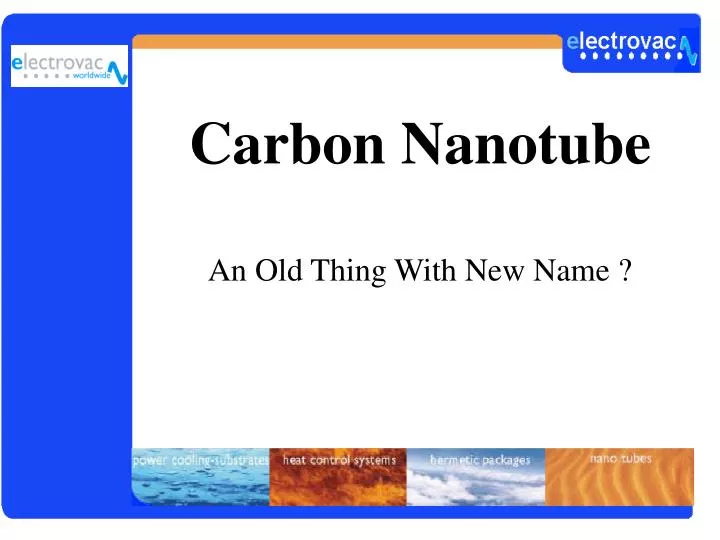
Carbon Nanotube An Old Thing With New Name ?. Carbon nanotube ?. C60-FULLERENE SINGLE WALL NANOTUBE. Carbon Nanotube Technology. Single Walled Carbon Nanotube SWNT. Multi Walled Carbon Nanotube MWNT. Fullerene Cap. 10-200 nm. 1.2 nm. Properties of Interest.

E N D
Carbon Nanotube An Old Thing With New Name ?
Carbon Nanotube Technology Single Walled Carbon Nanotube SWNT Multi Walled Carbon Nanotube MWNT Fullerene Cap 10-200 nm 1.2 nm
Properties of Interest • Resistivity 10-4cm • Maximum Current Density 1013 A/m2 • Thermal Conductivity ~ 2000 W/m/K • Young's Modulus (SWNT) ~ 1 TPa • Young's Modulus (MWNT) 1.28 TPa • Maximum Tensile Strength ~ 100 GPa
A BRIEF HISTORY OF CARBON NANOTUBES 1889 US Patent 405,480: Fe catalyst grows Carbon Fibers 1948 military interests in fibers and whiskers 1955 CVD synthesis of Carbon Nanofibers with Fe, Ni, Co 1976 Hollow tube structure of Carbon Nanofibers 1983 CCVD synthesis of hollow Carbon Nanofilaments 1991 Discovery of Carbon Nanotubes in Arc Discharge 1992- NANOTUBE GOLD RUSH: 500$/gramm 2001 Nanotube based FED 2002 NANOTUBE COMPOSITES, BATTERIES, TRANSISTOR 2018 NASA nanotube space elevator ?
Properties Arc Discharge Laser Ablation Chemical Vapor Deposition Nanotube generator Requires high-voltage arc discharge, not very expensive Requires high-power lasers, which are very expensive Carbon containing precursor vapors and catalysts, low cost Moving parts inside reaction chamber None Worm gear to reposition target at 1000 C None Precursor Solid carbon (graphite) Carbon target Carbon monoxide, acetylene, ethylene, xylene, etc. Process Batch – requires harvesting nanotubes Batch – requires changing targets and harvesting nanotubes Batch – direct deposition on product or harvesting for other applications Carrier gas Argon, helium Argon, helium Argon, nitrogen Diameters of nanotubes 1 – 10 nm 1 – 100 nm 1 – 1000 nm Length of nanotubes 0.01 – 0.1 µm 0.1 – 1 µm 1 – 1000 µm Yields ~ 50% ~ 70% ~ 60 – 90% Contaminants Soot, fullerenes, graphenes, amorphous carbon. High amount Fullerenes, amorphous carbon. Medium amount Almost none. Theoretically clean process Production quantities 10 g / day < 1 g / day 1 kg / day SUMMARY OF NANOTUBE PROCESS ROUTES
SUMMARY OF CATALYTIC CVD PROCESS Hydro-Carbon Catalyst Carbon-Layer carbides fishbone multiwalled soot
Thermionic cathode Electron sources of high intensity and high efficiency are desirable for a variety of applications. The most common electron source is the thermionic cathode such as the cathode-ray tube (CRT). The disadvantages of heating the cathode are the wasted energy and the relatively large minimum separation that can be reliably achieved between the cathode and current modulating electrodes.
Cold cathodes as the name implies, do not rely on the heating of a material to emit electrons over the vacuum barrier. There are several types of cold cathodes which can be classified based on their geometry. Field emitters rely on field enhancement created by sharp points or edges to facilitate tunneling of electrons. Planar cold cathodes fall into a large variety of types but in general do not rely on field enhancement for their operation.
Field Emitter as Cold Cathode The most common type of microelectronic cold cathode is the field emitter. Field emitters operate by tunnelling of electrons from a solid material into vacuum as the result of an impressed electric field. The high electric field serves to thin the vacuum barrier and allow electrons to tunnel. As the field emission process is dependent on a high electric field at the surface, a sharp, tip-like geometry is needed. Mo, W, Si and diamond are used as the Emitter. Field emission wastes no energy in the emission process and thus can approach 100% efficiency.
Three important Parameters of a Field Emitter The field enhancement factor: A high field enhancement will lower the applied voltage necessary for emission The emission area: It is determined by the geometry, and in general, it decreases as field enhancement is increased. One method to increase emission area without taking a large field enhancement penalty is to produce an array of field emitters The work function or electron affinity: the height of the barrier that the electrons must tunnel through, contributes to determining the operating voltage of the field emitter.
FED: field emission display The most commonly researched vacuum microelectronic display is the field emission display. In an FED, each pixel of the display is supplied electrons from an array of field emitters. The array of pixels on the screen is directly in front of the arrays of field emitters, and thus, the voltage necessary to excite the phosphors governs the required thickness of the display, with higher voltage phosphors requiring larger front-to-back spacing. The main components of the display are the cold cathode, the anode screen, and the spacers that separate the anode from the cathode. The cold cathode is composed of the field emitter arrays and the gate electrodes which turn on and off the emission for the individual pixels.
Cathode Ray Tube Field Emission Display L L large L = big housing small L = flat panel display Display technologies
Objective: patterned surface with discrete emission sites Field emission displays
Edge emitters Objective: patterned surface with discrete emission sites Bottom Up process: patterned growth • Negative photolithographic patterning of „forbidden“ sites • Graphitising of these sites • CVD process; decomposition of organometallic precursors • provide both catalyst and carbon from the gas phase • CNF grow on „positve“ sites CSIRO process:
Conventional field emitter for FEDs The first field emission electron sources were realized by the fabrication of microtips. The pioneer in the fabrication of vacuum microelectronic field emitter cathodes is Charles Spindt. The most common structure for microelectronic field emission cathodes now carries his name Pixtech, Motorola ,Futuba ,Samsung and Candescent Technologies had developed or already sold field emission displays (FEDs) based on microtips, which are usually made from silicon or molybdenum. Disadvantages of such cathodes: the expensive fabrication the threat of tip degradation due to the residual gas. The latter is especially a problem for applications where high emission current densities are required.
Pixtech: one of the famous company in this field In PixTech's field emission displays, electrons coming from millions of tiny microtips pass through gates and light up pixels on a screen. This principle is similar to that of cathode-ray tubes in television sets. The difference: Instead of just one "gun" spraying electrons against the inside of the screens face, there are as many as 500 million of them (microtips). PixTech designed, developed and manufactured field emission displays.The Company operated a display pilot manufacturing facility in France, R&D facilities and offices in the USA. It was developing high-volume manufacturing capabilities for its FEDs in Taiwan, and PixTech had also established a marketing partnership with Sumitomo Corporation. Unfortunately, it announced its bankruptcy a few months ago.
Challenges and Progresses on Carbon Nanotubes as Electron Field Emitter The ideal material for a field emitter would have high electron concentration, high thermal conductivity, and would be hard and non-reactive in the vacuum environment. High electron concentration is necessary for high emission current . A secondary concern for achieving high current density is the thermal conductivity of the emitter material. lifetime of field emitters is determined by the reactivity and mechanical strength of the emitter material. The advantages of the carbon nanotube as an electron field emitter tip include its small radius of curvature, high aspect ratio (L/R>100), low resistivity (10E-4Ohm-cm) , high thermal conductivity (~2000w/mK), high chemical resistance and strong mechanical strength. It has been shown that CNT is an excellent field emitter.
Fowler-Nordheim Equation Fowler-Nordheim formula for emission current J =k1E2 /ø exp(-k2 ø3/2/ E)E = U/ r J: Current density of field emission r: Size of tip ø: Work function By excellent electrical properties (lower work function, ø) as well as unique topology and structure (lower tip radius, r), carbon nanotube is an ideal field emitter.
Samsung announced the first 9-inch carbon-nanotube based FED The first 9-inch carbon nanotube based colour field emission displays (FEDs) are integrated using a paste squeeze technique. The panel is composed of 576 x 242 lines with implementation of low voltage phosphors. The uniform and moving images are achieved only at 2 V/µm. This demonstrates a turning point of nanotube for large area and full colour applications. The CNT-FEDs will be one of the very promising flat panel displays towards the new millenium.
Current EU Projects related to FED Carbon Nanotubes for Large Area Displays: CANADIS Project starting date: 31/08/2000 Deposition Equipment for Flat panel Display Fabrication: DEPODIS Project starting date: 01/09/2001 Printable Technologies for Consumer Priced Large Area Thin Flat Panel Color TV Display: PRINDIS Project starting date: 01/07/2001 Technologies and Advanced Materials for Kick-OFF in FED Manufacture: TAKEOFF Project starting date: 01/10/2001
Carbon nanotubes for large area displays Milestones of the CANADIS project:* In situ growth of localized CNT using CVD methods and catalyst. * Selection of the best method for reliable growth on large area substrate at low temperature. * Fabrication of a CVD reactor for growth of CNT on large area substrates. * Selection of the best triode structure for high performance FED. * Comparison between experimental data and theoretical models. * Modeling of field emission properties. * Fabrication of a 6' colored CNT based FED. * Fabrication of a 15' colored CNT based FED
Technologies and Advanced materials for Kick-OFF in FED Manufacture Carbon nanotubes on glass are used as the cathode. The direct deposition process is studied by two original routes: polymer-dispersed CNT deposited through a mask and chemical vapour deposition assisted by an extremely local heating. Cathodes using indirect CNT will be fabricated and tested in order to select the best option between the different gate technologies for triode-type FED: under-gate, remote-gate and normal-gate structures. The final packages cover the assembly of 18 inches CNT demonstrators and their final testing and evaluation. Samsung is one of the participaters.