Download
1 / 24
240 likes | 314 Vues
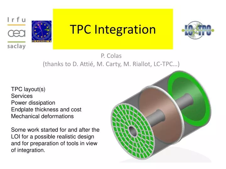
TPC Integration. TPC layout(s) Services Power dissipation Endplate thickness and cost Mechanical deformations Some work started for and after the LOI for a possible realistic design and for preparation of tools in view of integration. P. Colas

E N D
TPC Integration TPC layout(s) Services Power dissipation Endplate thickness and cost Mechanical deformations Some work started for and after the LOI for a possible realistic design and for preparation of tools in view of integration. P. Colas (thanks to D. Attié, M. Carty, M. Riallot, LC-TPC…)
Micromegas GEM Resistive foil necessary Bulk process avoids frames One high voltage 3x7 mm pads (or thinner at small R) Options: 2 GEMs, 3 GEMs Frames, at least in R Four or Six high voltages 1x5 mm pads • Very Both technologies being successfully tested in the EUDET facility at DESY. Technology has a serious impact on realistic design and integration. Still many R&D open questions : ion feedback, electronics,… TPC integration
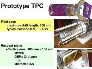
ILC-TPC Continuous 3D tracking in a large gaseous volume with O(100) space points. ILC-TPC (ILD concept) Large prototype being tested at DESY TPC integration
Micromegas GEM About 2000 readout channels AFTER-based electronics (made in Saclay) About 3200 readout channels ALTRO-based electronics (made at CERN) TPC integration
Micromegas DOUBLE GEM ‘Bulk’ technology (CERN-Saclay) with resistive anode (Carleton) New 100 micron GEM (plasma-etched in Japan) stretched from 2 sides. TPC integration
Micromegas DOUBLE GEM 4-layer routing (CERN) and 6-layer routing (Saclay) 24x72 pads, 2.7-3.2 mm x 7 mm 8-layer routing 28x176-192 pads, 1.1 mm x 5.6 mm TPC integration
Endplate panels Dimensions from ‘after-Cambridge’ Panel height 336 mm Panel width : from 278 to 454 About 6800 pads per panel TPC integration
Total weight 400kg per side (with Al) A design with 3 wheels also exists TPC integration
Micromegas 7-Module project • A completeprojectincluding software (alignment of the modules), integratedreadout, training for a pre-serie, tests and characterization in the T2K labat CERN. Very close to a real ILC Micromegas TPC (80 modules, 4 times larger, for eachside) • Electronicsdevelopment (at Saclay, with a verysignificant contribution from Canada): FEC, FEM, Backend. TPC integration
Front End Card Same as T2K (4 AFTER chips, 4x72 channels) but much less space In T2K, FECs are perpendicular to the pad plane Lot of space is taken by the protection (double diodes, decoupling capacitors and series resistors) : may be useless for ILC (Resistive foil protects). Tests are being performed to optimize these protections. Also lots of space taken by chip packaging (silicon is 7x7mm instead of 20x20 for the packaging ADC (one per card, 4 chips) can be moved to the FEM (one for all 24 chips) Connectors to the detector Connector to the FEM TPC integration
Front End Cards TPC integration
Front End Cards Minimal space: remove most of the protections, use naked chips wire-bonded on the FEC, transfer power regulation and ADC to the mezzanine module card. TPC integration
Front End Card 1 AFTER wafer purchased (300 good chips) Make 60 cards (36 good needed) Sent to ‘debugging’ and dicing end of this month. Bond chips (de-bonding possible). Chips can be tested only on cards. Repair cards with one dead chip. TPC integration
One per module, 1728 channels. Gathers signals from 6 FECs and sends it to the Back End through an optical link Front End Mezzanine 30 pins connector 30 pins connector 30 pins connector 30 pins connector 30 pins connector 30 pins connector SRAM ADC Xilinx Prom FPGA Xilinx V5 Optical connector Test Pulser 30 pins connector 30 pins connector 30 pins connector 30 pins connector 30 pins connector 30 pins connector TPC integration
Front End Mezzanine TPC integration
80 modules each side. For each module (6800 channels) : 1 HV cable 1 double optical fibre 1 low-voltage 32A cable 160 W to remove (becomes negligeable is power pulsing can be fully implemented. TPC integration
TPC Support 4 configurations Case 1 Case 2 Case 3 Case 4 TPC integration
TPC V1 - ∆P= 0 – Results Case 2 Case 1 Case 4 Case 3 TPC integration
TPC V1 - ∆P= 10 – Results Case 1 Case 2 Case 4 Case 3 TPC integration
TPC V1 vs V2 Déformation V1 - ∆P = 0 mbar Déformation V2 - ∆P = 0 mbar TPC integration
CONCLUSIONS A realistic design for the TPC is being worked on. It is very technology-dependent and still open questions need R&D (ion backflow, electronics). The work will be pursued with tools being prepared (M. Carty, R. Volkerborn, AIDA DESY-Saclay?) The Micromegas 7-module project should demonstrate the possibility of reading out the PCB with 30 mm - thick electronics, making a 100 mm endplate space possible. The bottleneck is now bringing Low-Voltage and removing heat (correlated problems). TPC integration