Download
1 / 17
200 likes | 408 Vues
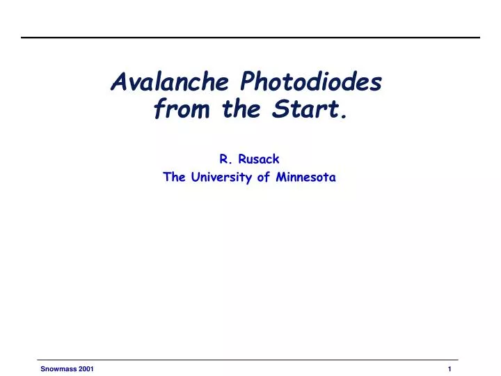
Avalanche Photodiodes from the Start. R. Rusack The University of Minnesota. Early History. Avalanche Photodiodes were invented by R. McIntyre at RCA in Canada in the late sixties. First considered in HEP at an Isabel meeting.

E N D
Avalanche Photodiodes from the Start. R. Rusack The University of Minnesota
Early History • Avalanche Photodiodes were invented by R. McIntyre at RCA in Canada in the late sixties. • First considered in HEP at an Isabel meeting. • Considered at the SDC for the readout of the EM shower max detector. • RCA ( GE EG&G) • API • RMD
- Ar coating Electric Field Collection Region h+ Si Avalanche region e p Contact layer Contact layer n Drift p Substrate ++ n + How they work Electrons generated by the incident light are multiplied in the high field region at the junction.
APD’s with crystals High side tail suppressed by APD.
APD’s in the CMS detector PbWO4 crystal
Light Output from PbWO4 Light out from Bogorodisk PbWO4 crystal. Output is peaked at 420 nm. ~50 photons/MeV from the
APD’s for CMS • Manufacturer: • Hamamatsu Photonics, Japan. • Quantity: • Two APD’s per crystal– 124,000 APD’s with spares. • Accessibility during operation: • None. • Radiation levels: • Maximum expected dose 200 kGy and 2 1013 neutrons/cm2. • Crystal Light Outout: • ~ 50 photons/MeV on a 4.5 cm2 area.
Basic APD Structure: Junction Si2N4 AR coating 5 ´ 5 mm2 active area Groove to minimize surface leakage current. APD is grown epitaxially on an n++ wafer.
APD parameters II Excess Noise Factor v Gain Capacitance v Bias Quantum Efficiency Response uniformity at 420 nm.
Problems Solved • Radiation Damage: • Neutron • Ionizing radiation. • API effect. • Quantum efficiency drift. • Change to epoxy • Lifetime: • Failure due to poor surface connectivity. • Electrical Characteristics. • High Capacitance.
Irradiation Tests. • Irradiation with protons: • All irradiation so far has been with an 70 MeV protons beam at PSI – Switzerland. • 2 1013 neutrons/cm2 in ~ 1 hour. • Irradiation with gammas. • All irradiation with 60C0 source. • Irradiation with neutrons. • Setting up a Californium source (252Cf) for irradiation at the University of Minnesota. • 2 1013 neutrons/cm2 in ~ 2 days.
Device failure Irradiation in a 70 MeV proton beam.
SiO2/SiN Al p++ n++ p n n++ Diagnosis Breakdown at this point when irradiated. High current at the SiO2-Al interface. Solution: increase spacing of Al deposit.
Lessons • To bring a new technology to reality requires: • Time 1987 to 1996. • Early resources. TNLRC/SSC to show viability. • To go from a possibility to an established technology takes: • Time 1996 to 2001. • Resources ~ $500k. • A manufacturer who sees this technology as a future money earner and does not expect to recover all costs of development from the experiment. • Expect the unexpected.