Download
1 / 1
10 likes | 118 Vues
4th International Conference on Materials for Advanced Technologies, Singapore July 1-6, 2007. New Negative Differential Resistance Device Design Suitable for Standard SiGe BiCMOS Nano-Technique. Kun Shan University. Department of Electronic Engineering. Student : Yi-Jhih Lin.

E N D
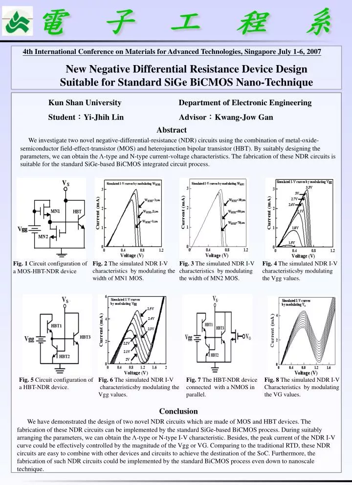
4th International Conference on Materials for Advanced Technologies, Singapore July 1-6, 2007 New Negative Differential Resistance Device Design Suitable for Standard SiGe BiCMOS Nano-Technique Kun Shan University Department of Electronic Engineering Student:Yi-Jhih Lin Advisor:Kwang-Jow Gan Abstract We investigate two novel negative-differential-resistance (NDR) circuits using the combination of metal-oxide-semiconductor field-effect-transistor (MOS) and heterojunction bipolar transistor (HBT). By suitably designing the parameters, we can obtain the Λ-type and N-type current-voltage characteristics. The fabrication of these NDR circuits is suitable for the standard SiGe-based BiCMOS integrated circuit process. Fig. 1 Circuit configuration of a MOS-HBT-NDR device Fig. 2 The simulated NDR I-V characteristics by modulating the width of MN1 MOS. Fig. 3 The simulated NDR I-V characteristics by modulating the width of MN2 MOS. Fig. 4 The simulated NDR I-V characteristicsby modulating the Vgg values. Fig. 5 Circuit configuration of a HBT-NDR device. Fig. 6 The simulated NDR I-V characteristicsby modulating the Vgg values. Fig. 7 The HBT-NDR device connected with a NMOS in parallel. Fig. 8 The simulated NDR I-V Characteristics by modulating the VG values. Conclusion We have demonstrated the design of two novel NDR circuits which are made of MOS and HBT devices. The fabrication of these NDR circuits can be implemented by the standard SiGe-based BiCMOS process. During suitably arranging the parameters, we can obtain the Λ-type or N-type I-V characteristic. Besides, the peak current of the NDR I-V curve could be effectively controlled by the magnitude of the Vgg or VG. Comparing to the traditional RTD, these NDR circuits are easy to combine with other devices and circuits to achieve the destination of the SoC. Furthermore, the fabrication of such NDR circuits could be implemented by the standard BiCMOS process even down to nanoscale technique.