Download
1 / 77
800 likes | 1.06k Vues
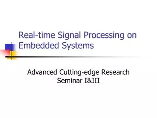
Real-time Signal Processing on Embedded Systems. Advanced Cutting-edge Research Seminar I&III. Recent Advances in Embedded Systems. Applications of classical embedded systems Factory Automation Electronic Calculator Applications of recent embedded systems Multimedia equipment Mobile Phone

E N D
Real-time Signal Processing on Embedded Systems Advanced Cutting-edge Research Seminar I&III
Recent Advances in Embedded Systems • Applications of classical embedded systems • Factory Automation • Electronic Calculator • Applications of recent embedded systems • Multimedia equipment • Mobile Phone • Video game console • etc Much computational power becomes indispensable.
Ex.1:Video Game Consoles • NES (Nintendo Entertainment System) • Ricoh 2A03 (8bit,MOS 6502-based) • SNES • Ricoh 5A22 (8/16bit,16MB address space) • Playstation • MIPS R3000 33.9MHz+ Geometric Transfer Engine • Playstation2 • Emotoin Engine 294-299 MHz, 6.2GFLOPS, 15W • Playstation3 • Cell Broadband Engine 3.2GHz 2TFLOPS, 60W
Ex.2:Handheld Game Consoles • Gameboy • Customized Z80 4MHz • Gameboy Advance • ARM7TDMI 16.7MHz/ Z80 4MHz • Nintendo DS/DS-Lite • ARM946E-S67 MHz/ARM7TDMI 33 MHz • Playstation Portable (PSP) • MIPS R4000 1-333MHz + Vector FPU 2.6GFLOPS @ 333MHz, 5GFLOPS Media Engine, Graphics Core
Features of embedded systems • Only strictly limited resources are available. • Memory spaces • Power consumption • Computing power • Reliability is required. • Real-time processing is indispensable.
Key technologies realizing recent high-performance embedded systems • Semiconductor integration technology • System implementation technology • SoC • SiP • Processor architecture • Speed up of IPC (Instructions Per Cycle) • Configurable processors • Multi-core processors
Improvement of integration density • Moore’sLaw: the number of transistors that can be placed inexpensively on an integrated circuit doubles approximately every two years. Adapted from Intel
MOS transistor • NMOS transistor gate channel Poly source drain SiO 2 n n Side view L P type substrate L: channel length Top view W W: channel width
Behaviour of NMOS • When input is given as shown in the figure, • Electrons are gathered under the gate.(This region is called channel.) V V DD in Poly SiO 2 - - - - - - - n n P type substrate
Behaviour of NMOS • When input is given as shown in the figure, • Then current can be conducted. V V DD in Poly SiO 2 - - - - - - - n n P type substrate
NMOS Inverter • Truth table V V V DD in out In Out
NMOS Inverter • Truth table V V= H V DD in out
NMOS Inverter • Truth table V V= H V DD in out
NMOS Inverter • Truth table V V= H V = L DD in out
NMOS Inverter • Truth table V V= L V DD in out
NMOS Inverter • Truth table V V= L V = H DD in out
PMOS transistor • PMOS is created on N-type substrate as shown in the figure. Poly SiO 2 p p N type substrate
PMOS transistor • If input is given as shown in the figure, • Holes are gatherd under the gate. Poly (<V ) V V V DD in DD DD SiO 2 + + + + + p p N type substrate
PMOS transistor • If input is given as shown in the figure, • Then current can be conducted. Poly (<V ) V V V DD in DD DD SiO 2 + + + + + p p N type substrate
PMOS Inverter • Truth table V V V DD in out
PMOS Inverter • Truth table V V =L V DD in out
PMOS Inverter • Truth table V V =L V DD in out
PMOS Inverter • Truth table V V =L V = H DD in out
PMOS Inverter • Truth table V V =H V DD in out
PMOS Inverter • Truth table V V =H V DD in out
PMOS Inverter • Truth table V V =H V = L DD in out
Characteristic of NMOS and PMOS • PMOS • can propagate H signal faster. • cannot propagate L signal so fast. • NMOS • can propagate L signal faster. • cannot propagate H signal so fast.
CMOS transistor • CMOS combines NMOS transistor and PMOS transistor complementally to improve performance. • Propagating H signal by PMOS. • Propagating L signal by NMOS. :P type diffusion layer : SiO : metal : Poly silicon 2 :N type diffusion layer N-Well P-Well PMOS NMOS
CMOS circuit • Ex: Inverter Diffusion layer (P type) Gate electrode (Poly silicon) V V V V V V V V DD SS DD in in SS out out : metal Diffusion layer (N type)
The size of the transistor • Performance of CMOS determined by channel width W and channel length L. • Several technological advances enable to create LSI circuits with very small L, generally known as “process rule”. • Small transistors enable high density implementation. • L is determined byfabrication accuracy. • Typical L is 0.25um, 0.18um, 65nm, 45nm, etc
Another CMOS circuits: NAND • Truth table B A Out A V V DD DD B A Out B
Another CMOS circuits: NAND • Truth table B=L A=L Out A=L V V DD DD B=L A Out B
Another CMOS circuits: NAND • Truth table B=L A=L Out A=L V V DD DD B=L A Out B
Another CMOS circuits: NAND • Truth table B=L A=L Out=H A=L V V DD DD B=L A Out B
Another CMOS circuits: NAND • Truth table B=H A=L Out A=L V V DD DD B=H A Out B
Another CMOS circuits: NAND • Truth table B=H A=L Out A=L V V DD DD B=H A Out B
Another CMOS circuits: NAND • Truth table B=H A=L Out=H A=L V V DD DD B=H A Out B
Another CMOS circuits: NAND • Truth table B=L A=H Out A=H V V DD DD B=L A Out B
Another CMOS circuits: NAND • Truth table B=L A=H Out A=H V V DD DD B=L A Out B
Another CMOS circuits: NAND • Truth table B=L A=H Out=H A=H V V DD DD B=L A Out B
Another CMOS circuits: NAND • Truth table B=H A=H Out A=H V V DD DD B=H A Out B
Another CMOS circuits: NAND • Truth table B=H A=H Out A=H V V DD DD B=H A Out B
Another CMOS circuits: NAND • Truth table B=H A=H Out=L A=H V V DD DD B=H A Out B
Recent digital LSI design scheme • LSI design flow System Spec Test Design System Design Layout Design Logic Design Mask creation Floor Plan Chip
Detail of the design flow • System Design • Defining architecture, SW/HW partitioning • Logic Design • RTL (Register Transfer Level) design by HDL. • Logic sysnthesis from RTL. • Floor Plan • Rough Place and Route. • Preliminary timing analysis (Gate level).
Detail of the design flow • Test Design • Inserting test circuits. • Layout Design • Gate level Place and Route. • Power line routing. • Layout verification. • Timing verification. (Gate level)
HDLs for digital design • What is HDL?: Hardware description Language. • Verilog: Developed by Cadence for Verilog-XL simulator. • VHDL: Developed by DARPA. It can support several abstraction levels of a function. • SFL: Structural Functional Language, Developed by NTT. It supports only single clock synchronous circuits.
Logic synthesis from HDL • You can obtain logic circuit from HDL by using synthesis tools such as design compiler.