Download
1 / 25
280 likes | 456 Vues
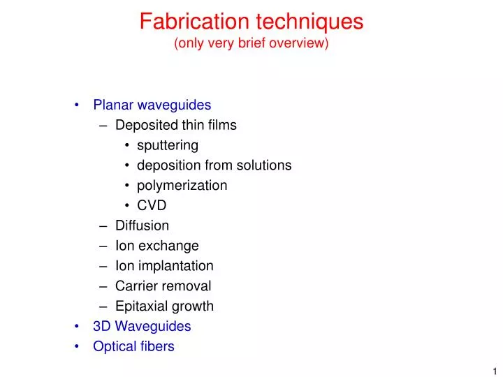
Fabrication techniques (only very brief overview). Planar waveguides Deposited thin films sputtering deposition from solutions polymerization CVD Diffusion Ion exchange Ion implantation Carrier removal Epitaxial growth 3D Waveguides Optical fibers. monolitické OIC.

E N D
Fabrication techniques(only very brief overview) • Planar waveguides • Deposited thin films • sputtering • deposition from solutions • polymerization • CVD • Diffusion • Ion exchange • Ion implantation • Carrier removal • Epitaxial growth • 3D Waveguides • Optical fibers
monolitické OIC α ~ 2 dB/cm (vlnovod) (GaInAsP 1.3/1.55 μm - „telekomunikační“ vlnové délky) jen hybridní OIC α < 0.3 dB/cm (vlnovod)
Sputtering e.g.plasma discharge vacuum (2-20).10-3 torr inert gas glass, KDP, Si...
Sputtering e.g. ion bean sputtering system
Diffusion Ti film
Ion exchange ~300°
Carrier removal • free carriers reduce the index of refraction • the cut-off condition is independent of wavelength GaAs, GaP
Epitaxial growth • fabrication of monolitic optical io formed on a semiconductor substrate • required bangap:
Molecular beam epitaxy (MBE) e.g.GaAlAsorGaInAsP
Optical fibers CVD:
1st step: preform fabrication using MCVD SiCl4 + O2 dopants


![Brief [ briefer , briefest ] ( adjective )](https://cdn1.slideserve.com/2610324/brief-briefer-briefest-adjective-dt.jpg)