Download
1 / 29
740 likes | 2.37k Vues
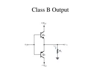
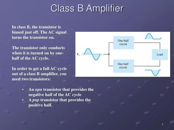
Class B Amplifier. In class B, the transistor is biased just off. The AC signal turns the transistor on. The transistor only conducts when it is turned on by one-half of the AC cycle. In order to get a full AC cycle out of a class B amplifier, you need two transistors:.

E N D
Class B Amplifier In class B, the transistor is biased just off. The AC signal turns the transistor on. The transistor only conducts when it is turned on by one-half of the AC cycle. In order to get a full AC cycle out of a class B amplifier, you need two transistors: • An npn transistor that provides the negative half of the AC cycle • A pnp transistor that provides the positive half.
Class B Amplifier • Since one part of the circuit pushes the signal high during one half-cycle and the other part pulls the signal low during the other half cycle, the circuit is referred to as a push-pull circuit
Input DC power • The power supplied to the load by an amplifier is drawn from the power supply • The amount of this DC power is calculated using • The DC current drawn from the source is the average value of the current delivered to the load
Input DC power • The current drawn from a single DC supply has the form of a full wave rectified signal, while that drawn from two power supplies has the form of half-wave rectified signal from each supply • On either case the average value for the current is given by • The input power can be written as
Output AC power • The power delivered to the load can be calculated using the following equation • The efficiency of the amplifier is given by • Not that • Therefore the efficiency can be re-expressed as
Output AC power • The maximum efficiency can be obtained if • The value of this maximum efficiency will be
Power dissipated by the output transistors • The power dissipated by the output transistors as heat is given by • The power in each transistor is given by
Example Example 1: For class B amplifier providing a 20-V peak signal to a 16-Ω speaker and a power supply of VCC=30 V, determine the input power , output power and the efficiency Solution: The input power is given by The peak collector load current can be found from
Example Solution: The input power is The output power is given by The efficiency is
Maximum power dissipated by the output transistors • The maximum power dissipated by the two transistors occurs when the output voltage across the load is given by • The maximum power dissipation is given by
Example Example 2: For class B amplifier using a supply of VCC=30 V and driving a load of 16-Ω, determine the input power , output power and the efficiency Solution: The maximum output power is given by The maximum input power drawn from the supply is
Example Solution: The efficiency is given by The maximum power dissipated by each transistor is
Class B Amplifier circuits • A number of circuit arrangements can be used to realize class B amplifier • We will consider in this course two arrangements in particular • The first arrangement uses a single input signal fed to the input of two complementary transistors (complementary symmetry circuits) • The second arrangement uses two out of phase input signals of equal amplitudes feeded to the input of two similar NPN or PNP transistors (quasi-complementary push-pull amplifier)
Complementary symmetry circuitsfirst arrangement • This circuit uses both npn and pnp transistor to construct class B amplifier as shown to the left • One disadvantage of this circuit is the need for two separate voltage supplies
Complementary symmetry circuits • another disadvantage of this circuit is the resulting cross over distortion • Cross over distortion can be eliminated the by biasing the transistors in class AB operation where the transistors are biased to be on for slightly more than half a cycle
Complementary symmetry circuits • A more practical version of a push-pull circuit using complementary transistors is shown to the right • This circuit uses to complementary Darlington pair transistors to achieve larger current driving and lower output impedance
Second arrangement • As stated previously the second arrangement which uses two equal input signals of opposite phase has to be preceded by a phase inverting network as shown below
Quasi-complementary push pull amplifier second arrangement • In practical power amplifier circuits it is preferable to uses npn for both transistors • Since the push pull connection requires complementary devices, a pnp high power transistor must be used. • This can be achieved by using the circuit shown
Example Example: For the circuit shown, calculate the input power, output power and the power handled by each transistor and the efficiency if the input signal is 12 Vrms Solution: The peak input voltage is The output power is
Example Solution: The peak load current is The dc current can be found from the peak as The input power is given by The power dissipated by each transistor is given by
Crossover Distortion If the transistors Q1 and Q2 do not turn on and off at exactly the same time, then there is a gap in the output voltage.
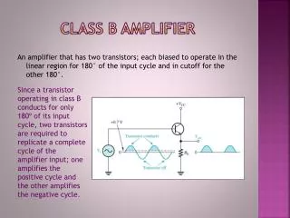
Class B Amplifier Push-Pull Operation • During the positive half-cycle of the AC input, transistor Q1 (npn) is conducting and Q2 (pnp) is off. • During the negative half-cycle of the AC input, transistor Q2 (pnp) is conducting and Q1 (npn) is off. Each transistor produces one-half of an AC cycle. The transformer combines the two outputs to form a full AC cycle. This circuit is less commonly used in modern circuits
Amplifier Distortion If the output of an amplifier is not a complete AC sine wave, then it is distorting the output. The amplifier is non-linear. This distortion can be analyzed using Fourier analysis. In Fourier analysis, any distorted periodic waveform can be broken down into frequency components. These components are harmonics of the fundamental frequency.
Harmonics • Harmonics are integer multiples of a fundamental frequency. • If the fundamental frequency is 5kHz: • 1st harmonic1 x 5kHz • 2nd harmonic 2 x 5kHz • 3rd harmonic 3 x 5kHz • 4th harmonic 4 x 5kHz • etc. • Note that the 1st and 3rd harmonics are called odd harmonics and the 2nd and 4th are called even harmonics
Harmonic Distortion According to Fourier analysis, if a signal is not purely sinusoidal, then it contains harmonics. 26
Harmonic Distortion Calculations Harmonic distortion (D) can be calculated: • where • A1 is the amplitude of the fundamental frequency • An is the amplitude of the highest harmonic The total harmonic distortion (THD) is determined by:
Power Transistor Derating Curve Power transistors dissipate a lot of power in heat. This can be destructive to the amplifier as well as to surrounding components.