Download
1 / 66
1.77k likes | 3.44k Vues
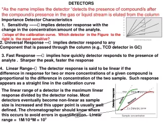
Optical Detectors. Abdul Rehman. Optical Detector Optical detector is an essential component of an optical receiver which converts received optical signal into an electrical signal. Improvement of detector characteristics and performance

E N D
Optical Detectors Abdul Rehman
Optical Detector Optical detector is an essential component of an optical receiver which converts received optical signal into an electrical signal. Improvement of detector characteristics and performance improves the link performance allowing fewer repeaters. Optical detector has the same required characteristics as that for the optical source Abdul Rehman Optical Communication
Requirements High sensitivity at operating wavelength High fidelity Large electrical response to received optical signal (high eff) Fast response/ short response time Low noise High stability Low cost Low bias voltages High reliability Small size
General Concept lC If the energy hν of the incident photon exceeds the band gap energy (hν > Eg) an electron-hole pair is generated each time a photon is absorbed by the semiconductor • Under the influence of an electric field set up by an applied voltage electrons and holes are swept across the semiconductor resulting in a flow of electric current
Responsivity The photo current Ipis directly proportional to the incident optical power Pin Ip= RPin Where R is resposivity of photodetector in units of A/W output photo current I p incident optical power Pin R = = Responsivity is the ratio of the electrical output to the optical input. Abdul Rehman Optical Communication
Three fundamental processes occurring between the two energy states of an atom: (a) absorption; (b) spontaneous emission; and (c) stimulated emission. Abdul Rehman Optical Communication
Quantum Efficieny • The responsivity can be expressed in terms of Quantum efficiency electron generation rate = photon incidence rate η (Q E ) is a figure given for a photosensitive device (charge-coupled device (C C D ), for example) which is the percentage of photons hitting the photo reactive surface that w ill produce an electron-hole pair. It is an accurate measurement of the device's sensitivity. Energy of a photon is ' hν ' so the photon incident rate may be written Piin in terms of incident optical power and the photon energy as Abdul Rehman hν Optical Communication
I p electron generation rate is given as q So Quantum efficiency can be written as • hn I p q Pin I p q Pin hn η = = ⋅ hν q I p = [since R = ] R Pin Abdul Rehman Optical Communication
ηq ηq = c = ηqλ ηλ = hc q R = hv h λ hc −6 η⋅ λ ⋅10-6.624*10−34 Js2.998*108 m s 1.602*10−19 C η⋅ λ ⋅10−6 ⋅1.602*10−19 m ⋅ C C 1 6.624*10 r 2.998*10 Js ⋅ s s j s = = ⋅ = x −34 8 m η⋅ λ 1.24 = • A W, where λis in µm Optical Communication Abdul Rehman
R ∝ λ until hν < E g because more photons are present for the same optical power This linear dependence on λ is not continue forever since eventually the photon energy becomes too small to generate electrons. • hv< Eg, The quantum efficiency η then drops to zero If the facets of the semiconductor slab are assumed to have an antireflection coating, the power transmitted through the slab of This happens for width W is ptr= exp(-αW ) pin Where α is absorption coefficient Abdul Rehman Optical Communication
The absorbed power is thus given by pabs= pin - ptr= [1 - exp(- α W)] pin Since each absorbed photon creates an electron-hole pair, the quantum efficiency η is given by pabs = 1 - exp ( -αW ) η= pin • η becomes 'zero' when α = 0. On the other hand ηapproaches 1 if αW>> 1 Abdul Rehman Optical Communication
The wavelength c at which αbecomes zero is called cutoff wavelength The material can be used as a photodetector only for < c Indirect – bandgap semiconductors: Si, Ge The absorption is not as sharp as for direct band-bandgap materials Direct – bandgap semiconductors : GaAs, InGaAs Abdul Rehman Optical Communication
Energy of incident photon must be greater than or equal to bandgap energy of the photodetector material. Therefore photon energy h c λ h c E g h ν ≥ E g ⇒ ≥ E g ⇒ λ ≤ Thus the threshold for detection commonly known as the long wavelength cutoff point λ c is h c E g λ c = This gives the longest wavelength of light for photodetection Abdul Rehman Optical Communication
Direct and Indirect Absorption(senior 425) Si and Ge absorbs light by both direct and indirect optical transitions . Indirect absorption requires the assistance of a photon so that momentum as well as energy are conserved. For direct absorption no photon is involved so transition probability is more likely. Si is only weakly absorbing over the wavelength band of interest in optical fiber communications (800-900 nm). For Ge the threshold for direct absorption occurs above 1530 nm and Ge may be used in the fabrication of the detectors over the whole of the wavelength range of interest. Photodiode material should be chosen with bangap energy slightly less than the photon energy corresponding to the longest operating wavelength of the system.
This gives a sufficiently high absorption coefficient to ensure a good response and at the same time limits the thermally generated carriers in order to achieve a low dark current Ge diodes have relatively large dark currents - a disadvantage of Ge To overcome this problem certain alloys of Ge are made where the bandgap is adjusted as per the requirements like InGaAs, GaAlSb Abdul Rehman Optical Communication
Bandwidth(agrawallll 135) The bandwidth of photodetector is determined by the speed with which it responds to variation in the incident optical power. The rise time is defined as time over which the current builds up from 10 % to 90 % of its final value when the incident optical power is changed abruptly. The rise time is written as; • Tr= (ln 9)(tr+ RC ) time constant transit time Abdul Rehman Optical Communication
The transit time is added to time constant of equivalent RC circuit because it takes some time before the carriers are collected after their generation through absorption of photons. The maximum collection time just equal to the time an electron takes to traverse the absorption region. The transit time can be reduced by decreasing W but the quantum efficiency begins to decrease significantly for αW < 3 Thus, there is a trade-off between the bandwidth and the responsivity (speed versus sensitivity) of a photodetector. Abdul Rehman Optical Communication
Thus there is trade-off between the bandwidth and the responsivity (speed versus sensitivity) of a photodetector. The bandwidth is given as 1 • 2(tr +RC ) Optical Communication f = Abdul Rehman
Rise and fall times Abdul Rehman Optical Communication
Dark current Id Dark current is the current generated in absence of optical signal It originates from: stray light thermally generated electron – hole pairs Id should be negligible for a good photodetector (Id<10nA) • • Abdul Rehman Optical Communication
4.2. Photodetector design Photodetectors can be broadly classified into two categories photoconductive photovoltaic Photoconductive detector homogeneous semiconductor slab as shown in fig before Little current flows when no light is incident Incident light increases conductivity through electron-hole generation and current flow is proportional to the optical power reverse biased p-n junction Photovoltaic detectors solar cells, produce voltage in the presence of light • – – • – – – – • – Abdul Rehman Optical Communication
p-n photodiodes A reverse bias p-n junction consists of a region, known as depletion region Electron-hole pairs are created through absorption when such p-n junction is illuminated with light on one side Because of the large built-in electric field, electrons and holes generated inside the depletion region accelerate opposite directions and drift to n and p sides respectively. The resulting flow of current is proportional to the incident optical power A reverse bias pn junction acts as a photodetector and is referred as pn photodiode Figure showing structure of a p-n photodiode Light is falling on one side of the photodiode (p-side) The depletion region has width W Abdul Rehman Optical Communication
As shown in the figure incident light is absorbed mostly inside the depletion region The responsivity of photodiode is quite high (R~1 A/W) because of high quantum efficiency The electron-hole pairs generated experiences a large electric field and drift rapidly towards the p or n side, depending on the electric charge The resulting current flow because of incident optical power I p = RPin
Bandwidth often limited by transit time .If W is the width of the depletion region and vd is the drift velocity, the transit time is given by W vd tr= m W = 10m , Vd =0 5 s 10 ⋅ 10 −6 m 10 s = 10 −10 s = 100ps tr= 5 m Good enough to 1 Gbit/s Abdul Rehman Optical Communication
Both W and Vdcan be optimized to minimize tr The depletion-layer width depends on the acceptor and donor concentrations and can be controlled through them. The velocity Vddepends on the applied voltage but attains a maximum value called saturation velocity ~ 105 m/s that depends on the material used. Abdul Rehman Optical Communication
Limiting factor Limiting factor for the bandwidth of p-n photodiode is the presence of a diffusive component in the photocurrent. The physical origin of diffusive component is related to the absorption of incident light outside the depletion region. Electrons generated in the p-region have to diffuse to the depletion-region boundary before they can drift to the n-side, similarly holes generated in the n-region must diffuse to the depletion-region boundary. Diffusion is an inherently slow process; carriers take a nanosecond or longer to diffuse over a distance of about 1 µm. Abdul Rehman Optical Communication
Figure shows how the presence of a diffusive component can distort the temporal response of a photodiode. The diffusion contribution can be reduced by decreasing the widths of the p- and n-regions and increasing the depletion- region width so that most of the incident optical power is absorbed inside it. This is the approach adopted for p–i–n photodiodes. Abdul Rehman Optical Communication
p-i-n energy-band diagram Abdul Rehman Optical Communication
p-i-n photodiodes A simple way to increase the depletion region width is to insert a layer of undoped or lightly doped semiconductor material between the p-n junction Since the middle layer consists of nearly intrinsic material so such a structure is referred as p-i-n photodiode Because of its intrinsic nature the middle i-layer a large electric field exists in the i-layer. The depletion region extends throughout the i-region and its width W can be controlled by changing the i-layer thickness
Most power is absorbed in i-region so drift dominates over diffusion The width W depends on a compromise between speed and sensitivity. The responsivity can be increased by increasing W so that quantum efficiency approaches 100% but at the same time the response time also increases as it takes longer time for carriers to drift across the depletion region. Optimum W is a compromise between responsivity and response time.
(PAGE 139 AGRAWAL) For indirect Si and GeW = 20 - 50m, for reasonable quantum efficiency The bandwidth of such photodiode is limited by relatively long transit time, tr> 200 ps By contrast in InGaAs,W=3 -5m that uses in direct bandgap semiconductor , the transit time is reduced So 10ps and the detector bandwidth 1 2πτ tr 10GHz, τ tr>> τ RC f 20 GHz possible, even 30 GHz with reduced η Abdul Rehman Optical Communication
Characteristics of common p-i-n diodes Symbol Unit µm Si 0.4-1.1 Ge 0,8-1,8 InGaAs 1,0-1,7 Parameter Wavelength λ R η Id A/W % nA 0,4-0,6 75-90 1-10 0,5-0,7 50-55 50-500 0,6-0,9 60-70 1-20 Responsivity Quantum efficiency Dark current τr Rise time ns 0,5-1 0,1-0,5 0,05-0,5 ∆f Vb Bandwidth Bias voltage GHz V 0,3-0,6 50-100 0,5-3 6-10 1-5 56 5-6
Intrinsic and extrinsic semiconductors An intrinsic semiconductor is one which is pure enough that impurities do not appreciably affect its electrical behavior. In this case, all carriers are created by thermally or optically excited electrons from the full valence band into the empty conduction band. Thus equal numbers of electrons and holes are present in an intrinsic semiconductor. Electrons and holes flow in opposite directions in an electric field, though they contribute to current in the same direction since they are oppositely charged. Abdul Rehman Optical Communication
N-type doping The purpose of n-type doping is to produce an abundance of mobile or "carrier" electrons in the material. To help understand how n-type doping is accomplished, consider the case of silicon (Si). Si atoms have four valence electrons, each of which is covalently bonded with one of four adjacent Si atoms. If an atom with five valence electrons, such as those from group VA of the periodic table (eg. phosphorus (P), arsenic (As), or antimony (Sb)), is incorporated into the crystal lattice in place of a Si atom, then that atom will have four covalent bonds and one unbonded electron. This extra electron is only weakly bound to the atom and can easily be excited into the conduction band. At normal temperatures, virtually all such electrons are excited into the conduction band. Since excitation of these electrons does not result in the formation of a hole, the number of electrons in such a material far exceeds the number of holes. In this case the electrons are the majority carriers and the holes are the minority carriers. Because the five- electron atoms have an extra electron to "donate", they are called donor atoms. Abdul Rehman Optical Communication
P-type doping The purpose of p-type doping is to create an abundance of holes. In the case of silicon, a trivalent atom (such as boron) is substituted into the crystal lattice. The result is that one electron is missing from one of the four covalent bonds normal for the silicon lattice. Thus the dopant atom can accept an electron from a neighboring atoms' covalent bond to complete the fourth bond. Such dopants are called acceptors. The dopant atom accepts an electron, causing the loss of one bond from the neighboring atom and resulting in the formation of a "hole." Each hole is associated with a nearby negative-charged dopant ion, and the semiconductor remains electrically neutral as a whole. However, once each hole has wandered away into the lattice, one proton in the atom at the hole's location will be "exposed" and no longer cancelled by an electron. For this reason a hole behaves as a quantity of positive charge. When a sufficiently large number of acceptor atoms are added, the holes greatly outnumber the thermally-excited electrons. Thus, the holes are the majority carriers, while electrons are the minority carriers in P-type materials. Blue diamonds (Type IIb), which contain boron (B) impurities, are an example of a naturally occurring P-type semiconductor. Abdul Rehman Optical Communication
Double-hetereostructure The performance of p-i-n photodiode can be improved considerably by using double- heterostructure design In this the middle i-type layer is sandwiched between the p- type and n-type layers of a different semiconductor whose bandgap is chosen such that light is absorbed in the middle i-layer A p-i-n photodiode commonly used for lightwave applications uses InGaAs for the middle layer and InP for the surrounding p-type and n- type layers. Abdul Rehman Optical Communication
Double – heterostructure design hc 6.626x10−34 x2.998x108 Eg 1.35x1.602x10 λ c = = = 0.92µm −19 InP: Eg=1.35 eV λC=0.92 µm (transparent for wavelengths greater than 0.92 µm) λC=1.65 µm InGaAs: Eg=0.75 eV lattice matched
The middle InGaAs layer absorbs strongly in the wavelength region 1.3-1.6 µm The diffusive component of the detector current is eliminated completely because light is only absorbed inside the depletion region The quantum efficiency η can be made almost 100% by using an InGaAs layer 4-5 µm thick Bandwidth as high as 70 GHz were realized using thin absorption layer (W< 1 µm) but only at the expense of a lower quantum efficiency η and responsivity By 1995 photodiodes exhibit bandwidth ∆f≈110 GHz and τRC ≈1ps
How to improve efficiency ?? Fabry-Perot cavity (laser like structure) can be formed around p-i-n structure to enhances quantum efficiency to ∼94%. FP cavity has a set of longitudinal modes at which the internal optical field is resonantly enhanced through constructive interference The result of such structure is that when the incident wavelength is close to longitudinal mode such photodiode exhibit high sensitivity
Another approach for efficient high-speed photodiodes is use of optical waveguide into which the optical signal is edge-coupled It enhances quantum efficiency to ∼100% as absorption takes place along the length of the optical waveguide (∼10 µm ) 50 Ghz bandwidth was realized in 1992 for waveguide photodiode. The bandwidth could be increased to 110 GHz by adopting mushroom-mesa waveguide structure. In this structure the width of the i-type absorbing layer was reduced to 1.5 µm while the p- and n- type cladding layers were made 6 µm wide In this way both parasitic capacitance and the internal series resistance were minimized, reducing TRC to about 1 ps ∆f ≈172 GHz η ≈ 45%
Speed of response The main factors limit the response of photodiode are Drift time of carriers through the depletion region Diffusion time of carriers generated outside the depletion region Time constant incurred by the capacitance of photodiode with its load Abdul Rehman Optical Communication
Avalanche photodiodes All detectors require a certain minimum current to operate reliably The current requirement translate into minimum power requirements through I p Pin = R • Detectors with large responsivity R are preferred since they require less optical power • The responsivity of p-i-n photodiode can takes its maximum value R = q for = 1 hν = --- q hv R Abdul Rehman Optical Communication
APDs can have much larger values of R as they are designed to provide an internal current gain They are used when the amount of optical power that can be spared for the receiver is limited The physical phenomenon behind the internal gain is known as impact ionization Under certain conditions, an accelerating electron can acquire sufficient energy to generate a new electron-hole pair Abdul Rehman Optical Communication
The energetic electron gives a part of its kinetic energy to another electron in the valence band that ends up in the conduction band, leaving behind a hole The net result of impact ionization a single primary electron, generated through absorption of a photon, creates many secondary electrons and holes, all of which contribute to photodiode current Abdul Rehman Optical Communication
The primary hole can also generate secondary electron-hole pairs that contribute to the current The generation rate is governed by two parameters, impact-ionization coefficient of electrons ,average number of electrons created per length αe: αh: holes, impact-ionization coefficient of average number of holes created per length The numerical value of e and h depends on the semiconductor material and on the electric field that accelerates electrons and holes
• In the last figure α e ⎫ ⎬ α h ⎪ ⎪ • 1⋅104 cm-1 ⇒ E =2 -4 ×10 V cm 5 ⎭ These values can be realized by applying a high voltage (∼100 V) to the APD APDs differ in their design from that of p-i-n photodiodes is that an additional layer is added in which secondary electron-hole pairs are generated through impact ionization Abdul Rehman Optical Communication