Download
1 / 62
620 likes | 630 Vues
Designing electronics for a TOF Forward PID for SuperB D.Breton & J.Maalmi (LAL Orsay), E.Delagnes (CEA/IRFU). Introduction.

E N D
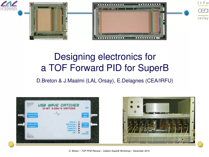
Designing electronics for a TOF Forward PID for SuperBD.Breton & J.Maalmi (LAL Orsay), E.Delagnes (CEA/IRFU)
Introduction In the view of the TOF FPID solution for SuperB, we have installed a test setup at SLAC in order to estimate our ability to measure the time of flight of muons between two quartz bars with a sufficient precision. To this end, we have developped dedicated electronics on the base of an existent module called WaveCatcher. The two-bar setup is rather simple, but the capacity for electronics to measure all channels simultaneously with a 10ps time precision is not. => we will describe the state of the art for high precision time measurement => we will explain here why we think analog memories are the right solution for this type of measurement => we will describe the WaveCatcher module => we will present the current 16-channel setup and how we intend to move toward prototyping a 672-channel system
About TDCs … Existing electronics for time measurement is mostly based on Time to Digital Converters (TDC). A TDC converts the arrival time of a binary signal into digital value. Very few products on the market, mostly dedicated to LHC HPTDC from CERN => 25ps & 40MHz TDC-GPX from ACAM => 8 channels, 80ps & 40MHz There is an important demand for time of flight measurement in the medical community We are currently developping for the barrel PID a 16-channel chip (SCATS) with high counting rate capability and very simple way of use: 160MHz clock (130-200), 200ps step, resolution of 70ps, data-push (triggerless), up to 5 MHz counting rate for all channels, input dead time < 50ns Low power, very cheap (CMOS 0.35µm) BUT a TDC needs a binary input signal • analog input signal has to be translated to digital with a discriminator • overall timing resolution is given by the quadratic sum of the discrimator and TDC timing resolutions
To feed the TDC, one needs to transform analog pulse into digital without jitter => this is commonly done with a Constant Fraction Discriminator (CFD) Indeed, a simple threshold method introduces Time Walk which depends on the signal amplitude Time can be corrected but this implies implementing the measurement of the amplitude in addition to that of the time in order to remove the time walk, threshold has to be set as a constant fraction of the amplitude State of the art: CFD (1) A1 V V relative threshold : constant fraction of the peak! A2 A3 k x A1 Fixed threshold k x A2 k x A3 t t Δt : time walk Δt ~ 0
State of the art: CFD (2) The drawing below describes how to produce a digital edge at a constant fraction of an analog pulse => the implementation with analog electronics looks easy at first order Δ V S(t) S(t- Δ) S(t) S(t- Δ) Δ + comp k x S(t) - k k x A t Δ A S(t- Δ) > k .S(t) • Difficulty: • Delay has to be adapted to pulse rise-time • Ratio has to be adjusted to maximum slope • both Δ and k have to be programmable • And …
State of the art: CFD (3) Moreover, in order to avoid triggering on the noise, the system has to be armed by a first threshold => the easiest implementation with analog electronics: zero crossing method Δ V S(t) S(t- Δ) k x A S(t- Δ) – k x S(t) k x S(t) S(t) S(t- Δ) t Δ + + Σ k x S(t) Zero-crossing instant Arming threshold comp - k - Arming threshold A S(t- Δ) – k.S(t) > 0 • Problem : one cannot implement a pure delay line in an ASIC. • => delay is usually made of: • cascaded R-C cells => signal is deformed • or specific shaping => very sensitive to pulse shape • There is always some remaining dependence on transit time to amplitude • >> Time resolution of ASICs based on CFD/TDC solution : > 30 ps rms
State of the art: digitization Extraction of the time canbeperformedthanks to a digital treatment of the digitized signal (waveformsampling). Different types of algorithmscanbeused A simple and stillveryperforming solution is a digital CFD Analog to Digital Converters : An ADC converts an instantaneous voltage into digital value. The mostpowerfulproducts on the market: 8bits => 3GS/s, 1,9 W => 24Gbits/s, 10 bits => 3GS/s, 3,6 W => 30Gbits/s 12 bits => 3,6GS/s, 4,1 W => 43,2Gbits/s 14 bits => 400MS/s, 2,5 W => 5,6Gbits/s => Collateraldammages : their package, consumed power, output data rate ! => appearance of integratedcircularbuffers (limited by technology) BGA 292 pins 24x1,8Gbits/s
About digitization boards … Designing a board with an ADC producing tens of Gbits/s is a huge effort High-end FPGAs have to be used If one wants to record some time depth, banks of DDR3 RAMs have to be used A few companies started the exercise These boards are expensive (5 to 40 k$) and house very few channels (the most often 2 sharing the ADC and thus the GS/s) This is perfect for very high precision and very little scale, and for systems where dead-time before digitization is critical This is more a problem for high scale and low power … Moreover, very fast ADC often use parallelized architecture, which is not good for signal uniformity …
Some ADC boards … (1) PX1500-4: 3 GSPS 8-bit ADC and Virtex-5 Processing PCI Express 8x Module ADC10D1500RB: a Low-Power, 10-Bit, Dual 1.5 GSPS or Single 3.0 GSPS A/D Converter Reference Board
Some ADC boards … (2) ADC12D1800RB: 12-Bit, Dual 1.8 GSPS or Single 3.6 GSPS A/D Converter Reference Board XMC-1151: 3.2 GSPS 12-bit ADC and Virtex-6 Processing XMC PCI Express Module
Why Analog Memories ? Analog memories actually look like perfect candidates for high precision time measurements at high scale: Like ADCs they catch the signal waveform (this can also be very useful for debug) There is no need for precise discriminators TDC is built-in (position in the memory gives the time) Only the useful information is digitized (vs ADCs) => low power Any type of digital processing can be used Only a few samples/hit are necessary => this limits the dead time Simultaneous write/read operation is feasible, which may further reduces the dead time if necessary But they have to be carefully designed to reach the necessary level of performance …
Short history of the Orsay/Saclay SCA Developments • The story begins in 1992 with the design of the first prototype of the Switched Capacitor Array (SCA) for the ATLAS LARG calorimeter. After 10 years of development, the main final characteristics of this rad-hard circuit were: • 12 pseudo-differential channels • 40 MHz sampling • 13.6-bit dynamic range with simultaneous write/read • 80000 chips produced in 2002 and mounted on the detector. • Since 2002, 3 new generations of fast samplers have been • designed (ARS, MATACQ, SAM): total of more than30000 chips in use. • Our design philosophy: • 1. Maximize dynamic range and minimize signal distorsion. • 2. Minimize need for calibrations and off-chip data corrections. • 3. Minimize costs (both for development & production): • Use of inexpensive pure CMOS technologies (0.8µm then 0.35µm); • Use of packaged chips (cheap QFP). HAMAC
Principle of recording. • Clock virtually multiplied by 16 inside the chip. • Sampling Frequency servo-controlled inside the chip => no sensitivity to temperature & process variation. • Used as a circular buffer . • Area of interest readout: • Starting from Trigger cell (marked by trailing edge of the run signal) + programmable offset. • Total readout also possible. • Read Cell index available. • Low dead time due to readout • (<100ns / sample).
The SAM (Swift Analog Memory) chip • 2 differential channels • 256 cells per channel • BW > 250 MHz • Sampling Freq:700MHz-2.5GHz • High Readout Speed >16 MHz • Smart Read pointer (integrate a 1/Fs step TDC) • Few external signals • Many modes configurable by a serial link. • Auto-configuration @ power on • Low cost for medium size prod=> AMS 0.35 µm • This chip was first designed for HESS2 experiment: • a big Athmospheric Cerenkov Telescope • located in the Namibia desert. NIM A, Volume 567, Issue 1, p. 21-26, 2006 6000 ASICs delivered in Q2 2007, yield of 95%.
The new SAMLONG ASIC • SAM was a great demonstrator for precision time measurement. • But in parallel there was a need for longer depth analog memories • A chip like SAM with 1024 cells and compatible with the WaveCatcherboard was designed: SAMLONG. This chip also includes: • a ramp TDC (“vernier”) for tagging the trigger arrival time (like in our former MATACQ chip). • New input buffers (slew rate, power) • New readout amplifiers (noise) • Output multiplexor (single ADC) • Internal programmable posttrig • Target: same performances as SAM but with less power (300mW => 200mW / 2ch) • Everything we learnt from SAM for time precision was taken into account • SAMLONG was submitted in April 2010 and received in September • It was mounted on a WaveCatcher V4 and worked immediatly! • It is a fruitful source of informations for the future design of a new chip optimized for time measurement …
The WaveCatcher module : short description and performances.
The USB Wave Catcher board V5 Reference clock: 200MHz => 3.2GS/s Pulsers for reflectometry applications Board has to be USB powered => power consumption < 2.5W 1.5 GHz BW amplifier. 480Mbits/s USB interface µ USB Trigger input 2 analog inputs. DC Coupled. Clock input Trigger output +5V Jack plug Trigger discriminators Cyclone FPGA SAM Chip Dual 12-bit ADC
Possibility to add a individual DC offset on each signal Individual trigger threshold on eachchannel External and internal trigger + numerous modes of triggering on coïncidence (11 possibilitiesincludingtwo pulses on the samechannel => useful for afterpulsestudies Embedded charge mode (integrationstarts on threshold or at a fixed location) => high rates (~ 3.5 kEvents/s) Pulse generators for reflectometry applications Externalclock input for multi-board applications BoardSpecialFeatures
5 versions of the boardsince sept 2008 … V2 V1 V6 is on its way … V3 V4 V5
Description of the time measurement setup Open cable USB Wave Catcher USB Wave Catcher USB Wave Catcher • For the least jitter at short distance … Two pulses on different channels or boards Two pulses on the same channel => with this setup, we can measure precisely the time difference between the pulses independently of the timing characteristics of the generator! HP81110/12/12 • For other distances: high end generator • Two pulses generated with a programmable delay • Crosscheck with first method is performed at short distance
CVI acquisition software with GUI This software can be downloaded on the LAL web site at the following URL: http://electronique.lal.in2p3.fr/echanges/USBWaveCatcher/
Source: asynhronous pulse sent to the two channels with cables of different lengths or via a generator with programmable distance. Time difference between the two pulses extracted by digital CFD method. Threshold determined by polynomial interpolation of the neighboring points. Pulses on different channels: CFD method Spline, extraction of the baseline, and normalization Threshold interpolation Ratio to peak 0.23 Time 0.23 Other method usable: Chi2 algorithm based on reference pulses.
Time measurement results : example with Δt ~ 0 WaveCatcher V4 : 2 pulses with Tr = Tf = 1.6ns and FWHM = 5ns Distance between pulses : Δt ~ 0 Differential jitter = 4.61ps 4.61psrms All matrix positions are hit!
Jitter vs Time distance betweentwo pulses Source: randomly distributed set of two positive pulses Results are the same with negative pulses or distance between arches of a sine wave Jitter distribution isalmost flat => good for use as TDC !
Effect of CFD ratio on time precision • WaveCatcher V4 : 2 pulses withTr = Tf = 1.6ns and FWHM = 5ns • Δt ~ 0 ns, - Δt ~ 10ns, - Δt ~ 20 ns Optimum value : corresponds to the maximum slope of the pulse!!
Characterization of 10µm- MCPPMT with the WaveCatcherBoard at SLAC Comparison with high-end standard electronics (NIM paper). D.Breton, E.Delagnes, J.Maalmi, K.Nishimura, L.L Ruckman, G.Varner & J.Va’vra
Fermilab beam test Jerry tested the adequation of 10µm MCPPMTs for time of flight measurements Conditions: ~40pe and low gain (2-3 104) Beam CFD with walk correction Raw CFD measurement
SLAC laser test Same conditions as for Fermilab test: 40pe and low gain (2-3 104) WaveCatcher Board 100Hz Tektronix oscilloscope
Two timing methods used (a) Software CFD method: (b) Reference pulse method : Average pulse shape used for the reference timing 2 algorithm (black is average, red shows ± 2 contour). • The first analysis step was to perform a spline interpolation of the waveform, which worked with either 1ps or 10ps time bins (in the end it was determined that 10ps binning is sufficient). Then two timing methods were used: • (a) One is a software CFD timing method, which consists of normalizing the pulses to the same peak amplitude and using a constant-fraction threshold, usually set to 18-22% of the peak amplitude. • (b) The second one, a reference timing method, in which one determines first a reference pulse shape. The pulse time is then determined by stepping through a chosen reference pulse, and calculating a 2 using a certain number of time bins.
Comparison of both methods Fig.2: Search for 2-minimum Fig.1: Reference pulses - fits to leading edge (a) TOF 1 (b) TOF 2 Fig.3: CFD vs. Reference timing Reference method: CFD method: • One can use, for example, a second order polynomial to fit only the leading edge of the average pulse profile for normalized pulses (see Fig.1). Fig.2 shows (a) the 2 values as a function of the time step, and (b) resulting time distributions correspond to a 2-minimum. • Figs. 3a&b show the final timing results for both (a) the reference timing method and (b) the CFD method.
SLAC test summary Sampling period! From this we could conclude that applying a very simple algorithm, which is very easy to integrate in a FPGA (finding a maximum & linear interpolation between two samples, i.e., without a use of the Spline fit) already gives very good results (only 10% higher than the best possible resolution limit).
SLAC test summary Summary of all the test results
NIM paper has been accepted in November Abstract:… There is a considerable interest to develop new time-of-flight detectors using, for example, micro-channel-plate photodetectors (MCP-PMTs). The question we pose in this paper is if new waveform digitizer ASICs, such as the WaveCatcher and TARGET, operating with a sampling rate of 2-3 GSa/s can compete with 1GHz BW CFD/TDC/ADC electronics ... … Conclusion: … The fact that we found waveform digitizing electronics capable of measuring timing resolutions similar to that of the best commercially-available Ortec CDF/TAC/ADC electronics is, we believe, a very significant result. It will help to advance the TOF technique in future.
Developments towards large scale implementation of analog memories for precise time measurement.
For the two-bar TOF test at SLAC, wedecided to build a synchronoussixteenchannel acquisition system based on 8 two-channelWaveCatcher V5 boards. Technical challenge: to keep the 10ps precisionat the cratelevel The system has to workwith a commonsynchronousclock There wetakebenefit of the externalclock input of the WaveCatcher V5 It is self-triggered but italso has to besynchronizedwith the rest of the CRT Rate of cosmicsislowthus computer time tagging of eventsisadequate (if all computers are finelysynchronized) Like the WaveCatcher, data acquisition isbased on 480Mbits/s USB. Introduction
Experimental setup Faraday cage 16 SMA connectors To amplifiers PM-side harness Patch panel MCPPMT µ Trigger for the electronics crate (QTZ3)
MCPPMT setup We grouped the pixels into 16 groups of 3 separated by 2 grounded pixels GROUNDED Equalization of the line lengths for each group of 3 pixels: 14.7 mm
36dB Amp 36dB Amp 36dB Amp 36dB Amp CH0 CH0 CH0 CH0 CH0 CH0 CH0 CH0 CH1 CH1 CH1 CH1 CH1 CH1 CH1 CH1 Clk in Clk in Clk in Clk in Clk in Clk in Clk in Clk in Trig out Trig out Trig out Trig out Trig out Trig out Trig out Trig out Trig in Trig in Trig in Trig in Trig in Trig in Trig in Trig in Trig out Trig out Trig out Trig out Trig out Trig out Trig out Trig out Electronics setup USB hub From QTZ3 8 16 amplifiers Patch panel USB Ext trig out Ext trig in USB USB USB USB USB USB USB USB Clk out 8 Trig out 8 Trig in 8 Clock and control board 8 USB WaveCatcher V5 DAQ PC
Clock and control board (1) From WaveCatchers To WaveCatchers From QTZ3 CRT mode : when the controllerboarddetects a coincidencebetween an external trigger from QTZ3 and one of the sixteenchannels, itsendsthrough USB a specificinterrupt to the PC in order to start the data readout.
Clock and control board (2) USB interface => 480Mbits/s Zero jitter clock buffer Clock outputs Trig outputs µ USB Trigger Input (NIM) Trigger Output (NIM) +5V Jack plug Pulse output Trig inputs Reference clock: 200MHz Cyclone FPGA
4-channel prototype • Succesfully tested at CERN mid July on new high speed MRPCs
Time performance of multi-board system Mean differential jitter is of about 12ps rms which corresponds to 8.5 ps rms of time precision per pulse
Comments about SLAC setup • Baseline uses sixteen individual 36 dB amplifiers but a solution with a board housing 16 amplifiers with programmable gain is under study • It could be used for the second step based on SL10 • This would anyhow be a very nice item on the shelf • Common trigger for the WaveCatcher boards is the signal produced by QTZ3: • This will stop the signal recording into the analog memory • but readout is performed only if at least one of the two-bar channels were hit (done through a OR of the individual triggers on signal) • Upon each event, the software adds the event time in the data file • => synchronization of events with the CRT µPC • time is regularly (once per minute) synchronized with SLAC time server (as µPC also does) via NTP time server.