Download
1 / 72
830 likes | 1.1k Vues
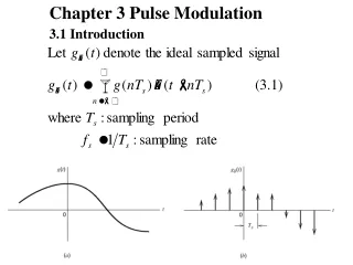
Chapter 3 Pulse Modulation 3.1 Introduction. 2. 3. 4. 5. Figure 3.3 ( a ) Spectrum of a signal. ( b ) Spectrum of an undersampled version of the signal exhibiting the aliasing phenomenon. 6.

E N D
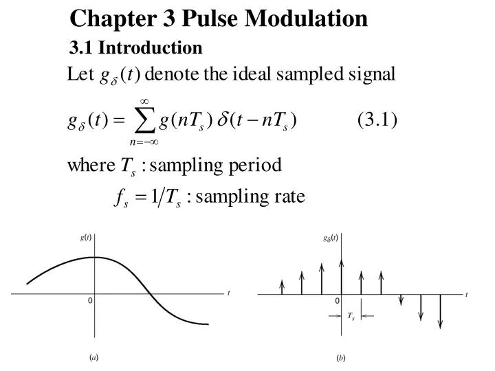
Chapter 3 Pulse Modulation 3.1 Introduction
Figure 3.3 (a) Spectrum of a signal. (b) Spectrum of an undersampled version of the signal exhibiting the aliasing phenomenon. 6
Figure 3.4 (a) Anti-alias filtered spectrum of an information-bearing signal. (b) Spectrum of instantaneously sampled version of the signal, assuming the use of a sampling rate greater than the Nyquist rate. (c) Magnitude response of reconstruction filter. 7
Pulse Amplitude Modulation – Natural and Flat-Top Sampling • The circuit of Figure 11-3 is used to illustrate pulse amplitude modulation (PAM). The FET is the switch used as a sampling gate. • When the FET is on, the analog voltage is shorted to ground; when off, the FET is essentially open, so that the analog signal sample appears at the output. • Op-amp 1 is a noninverting amplifier that isolates the analog input channel from the switching function.
Figure 11-3. Pulse amplitude modulator, natural sampling. Pulse Amplitude Modulation – Natural and Flat-Top Sampling
Pulse Amplitude Modulation – Natural and Flat-Top Sampling • Op-amp 2 is a high input-impedance voltage follower capable of driving low-impedance loads (high “fanout”). • The resistor R is used to limit the output current of op-amp 1 when the FET is “on” and provides a voltage division with rd of the FET. (rd, the drain-to-source resistance, is low but not zero)
Pulse Amplitude Modulation – Natural and Flat-Top Sampling • The most common technique for sampling voice in PCM systems is to a sample-and-hold circuit. • As seen in Figure 11-4, the instantaneous amplitude of the analog (voice) signal is held as a constant charge on a capacitor for the duration of the sampling period Ts. • This technique is useful for holding the sample constant while other processing is taking place, but it alters the frequency spectrum and introduces an error, called aperture error, resulting in an inability to recover exactly the original analog signal.
Pulse Amplitude Modulation – Natural and Flat-Top Sampling • The amount of error depends on how mach the analog changes during the holding time, called aperture time. • To estimate the maximum voltage error possible, determine the maximum slope of the analog signal and multiply it by the aperture time DT in Figure 11-4.
Figure 11-4. Sample-and-hold circuit and flat-top sampling. Pulse Amplitude Modulation – Natural and Flat-Top Sampling
Pulse Amplitude Modulation – Natural and Flat-Top Sampling Figure 11-5. Flat-top PAM signals.
Recovering the original message signal m(t) from PAM signal 10
3.4 Other Forms of Pulse Modulation a. Pulse-duration modulation (PDM) (PWM) b. Pulse-position modulation (PPM) PDM and PPM have a similar noise performance as FM. 11
Pulse Width and Pulse Position Modulation • In pulse width modulation (PWM), the width of each pulse is made directly proportional to the amplitude of the information signal. • In pulse position modulation, constant-width pulses are used, and the position or time of occurrence of each pulse from some reference time is made directly proportional to the amplitude of the information signal. • PWM and PPM are compared and contrasted to PAM in Figure 11-11.
Figure 11-11. Analog/pulse modulation signals. Pulse Width and Pulse Position Modulation
Pulse Width and Pulse Position Modulation • Figure 11-12 shows a PWM modulator. This circuit is simply a high-gain comparator that is switched on and off by the sawtooth waveform derived from a very stable-frequency oscillator. • Notice that the output will go to +Vcc the instant the analog signal exceeds the sawtooth voltage. • The output will go to -Vcc the instant the analog signal is less than the sawtooth voltage. With this circuit the average value of both inputs should be nearly the same. • This is easily achieved with equal value resistors to ground. Also the +V and –V values should not exceed Vcc.
Figure 11-12. Pulse width modulator. Pulse Width and Pulse Position Modulation analog 比較大時
Pulse Width and Pulse Position Modulation • A 710-type IC comparator can be used for positive-only output pulses that are also TTL compatible. PWM can also be produced by modulation of various voltage-controllable multivibrators. • One example is the popular 555 timer IC. Other (pulse output) VCOs, like the 566 and that of the 565 phase-locked loop IC, will produce PWM. • This points out the similarity of PWM to continuous analog FM. Indeed, PWM has the advantages of FM---constant amplitude and good noise immunity---and also its disadvantage---large bandwidth.
Demodulation • Since the width of each pulse in the PWM signal shown in Figure 11-13 is directly proportional to the amplitude of the modulating voltage. • The signal can be differentiated as shown in Figure 11-13 (to PPM in part a), then the positive pulses are used to start a ramp, and the negative clock pulses stop and reset the ramp. • This produces frequency-to-amplitude conversion (or equivalently, pulse width-to-amplitude conversion). • The variable-amplitude ramp pulses are then time-averaged (integrated) to recover the analog signal.
Figure 11-13. Pulse position modulator. Pulse Width and Pulse Position Modulation
Demodulation • As illustrated in Figure 11-14, a narrow clock pulse sets an RS flip-flop output high, and the next PPM pulses resets the output to zero. • The resulting signal, PWM, has an average voltage proportional to the time difference between the PPM pulses and the reference clock pulses. • Time-averaging (integration) of the output produces the analog variations. • PPM has the same disadvantage as continuous analog phase modulation: a coherent clock reference signal is necessary for demodulation. • The reference pulses can be transmitted along with the PPM signal.
Demodulation • This is achieved by full-wave rectifying the PPM pulses of Figure 11-13a, which has the effect of reversing the polarity of the negative (clock-rate) pulses. • Then an edge-triggered flipflop (J-K or D-type) can be used to accomplish the same function as the RS flip-flop of Figure 11-14, using the clock input. • The penalty is: more pulses/second will require greater bandwidth, and the pulse width limit the pulse deviations for a given pulse period.
Figure 11-14. PPM demodulator. Demodulation
Pulse Code Modulation (PCM) • Pulse code modulation (PCM) is produced by analog-to-digital conversion process. • As in the case of other pulse modulation techniques, the rate at which samples are taken and encoded must conform to the Nyquist sampling rate. • The sampling rate must be greater than, twice the highest frequency in the analog signal, fs > 2fA(max)
Figure 3.10 Two types of quantization: (a) midtread and (b) midrise. 13
Quantization Noise Figure 3.11 Illustration of the quantization process. (Adapted from Bennett, 1948, with permission of AT&T.) 14
Conditions for Optimality of scalar Quantizers Let m(t) be a message signal drawn from a stationary process M(t) -A m A m1= -A mL+1=A mk mk+1 for k=1,2,…., L The kth partition cell is defined as Jk: mk< m mk+1 for k=1,2,…., L d(m,vk): distortion measure for using vk to represent values inside Jk .
Pulse Code Modulation Figure 3.13 The basic elements of a PCM system.
Line codes: 1. Unipolar nonreturn-to-zero (NRZ) Signaling 2. Polar nonreturn-to-zero(NRZ) Signaling 3. Unipor nonreturn-to-zero (RZ) Signaling 4. Bipolar nonreturn-to-zero (BRZ) Signaling 5. Split-phase (Manchester code)
Page 39 Fig 1.6 Figure 3.15 Line codes for the electrical representations of binary data. (a) Unipolar NRZ signaling. (b) Polar NRZ signaling. (c) Unipolar RZ signaling. (d) Bipolar RZ signaling. (e) Split-phase or Manchester code.
Page 49 Fig 1.11
Differential Encoding (encode information in terms of signal transition; a transition is used to designate Symbol 0) Regeneration (reamplification, retiming, reshaping ) Two measure factors: bit error rate (BER) and jitter. Decoding and Filtering
3.8 Noise consideration in PCM systems (Channel noise, quantization noise) (will be discussed in Chapter 4)