Download
1 / 24
250 likes | 343 Vues
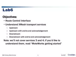
Lab6 On-Chip BUS Experiment. Speaker: Yu-Lin Hsiao Advisor: Prof. Chun-Yao Wang August 17, 2005. Department of Computer Science National Tsing Hua University. Outline. Introduction ﹣ Example 1 ﹣Example 2 Exercise. Experiment Task.

E N D
Lab6 On-Chip BUSExperiment Speaker: Yu-Lin Hsiao Advisor: Prof. Chun-Yao Wang August 17, 2005 Department of Computer Science National Tsing Hua University
Outline • Introduction ﹣Example 1 ﹣Example 2 • Exercise
Experiment Task • Flashes the LEDs on the Logic Module from left to right. • The speed of flashing the LEDs can be set by the 8-way switch. • FPGA version: program the FPGA by writing the bitstream image into the FPGA directly. The image will start running right after programming into the FPGA. • Flash version: program the FPGA by writing the bitstream into the flash. The image will start after next power up of the development system.
Step 1 • Create new project for Xilinx 4.1: (a) Device Family: VirtexE (b) Device: xcv2000e-6fg680 (c) Design Flow: XST Verilog
Step 2 • Add verilog file (Example1.v) to this project. Top module
Step 3 ★ ★ ★ • Copy user constraints file (example1.ucf) to the project directory and check the constraints. Name of user constraints file should be the same with top module!!
Step 4 • Generate the bitstream: ﹣Select Top module, ﹣Double click the Generate Programming File
Step 5 • Copy example1.bit to the directory which contains the progcards.exe file. (…/Codes/Hw/example1/download/) • Modify example1_to_flash.brd and example1_to_fpga.brd.
Step 6 • Connect ARM Multi-ICE onto LM, • Set the LM in Config Mode by shorting the CFGLNK jumper on the LM board. CFGLNK CFGLED
Step 7 • Auto-config in the Multi-ICE Server program.
Step 8 • Execute progcards.exe to download the bitstream to the FPGA.
Step 9 • Execute progcards.exe to download the bitstream to the Flash.
Step 10 • Set the LM in Normal Mode • Select the flash image to be executed. Which flash image to be executed is selected by the position of the 4-way switch S1 on the LM • Power the LM up again and observe the LM
Outline • Introduction ﹣Example 1 ﹣Example 2 • Exercise
Experiment Task • Determine DRAM size on the core module and sets up the system controller. • Check that the logic module is present in the AP expansion position. • Report module information. • Set the Logic Module clock frequencies. • Test SSRAM for word, halfword, and byte accesses. • Flash the LEDs. • Remain in a loop that displays the switch values on the LEDs.
Software (SW) • logic.c: The main C code. • logic.h: Constants. • platform.h: Constants. • rw_support.s: Assembler functions for SSRAM testing.
Phase 1 • Repeat step 1 to step 7, step 9, and step 10 above to download the bitstream (ahbahbtop.bit) to the Flash. • After finishing step 9, we have set LM in Normal Mode and selected the flash image to be executed by the 4-way switch. • Before powering up again, we first do phase 2.
Phase 2 (1/3) • Connect ARM Multi-ICE onto CM. • Power up and configure the Multi-ICE again.
Phase 2 (2/3) • Start CodeWarrior IDE. Open a new project and add the software code to this project.
Phase 2 (3/3) • Hit run bottom, it will start the AXD debugger.
Outline • Introduction ﹣Example 1 ﹣Example 2 • Exercise
Exercise • To trace the hardware code and software code, indicate that software how to communicate with hardware using the AMBA interface. • If we want to design an accumulator ( 1,2,3,… ), how could you do to implement it using the scratch code? • In example 1, explain the differences between the Flash version and the FPGA one.