Download
1 / 23
280 likes | 622 Vues
Introduction to Wafer fabrication. Process. Presented by Asst.Prof. Dr. Rardchawadee Silapunt. Outlines. Clean room. Wafer Fab Process. 1. 2. Outlines. Clean room. 1. Clean Room @ TMEC. It took time to install cleanroom. PLAY MOVIE. Outlines. Wafer Fab Process. 2. 6.

E N D
Introduction to Wafer fabrication Process Presented by Asst.Prof. Dr. Rardchawadee Silapunt
Outlines Clean room Wafer Fab Process 1 2
Outlines Clean room 1
It took time to install cleanroom PLAY MOVIE
Outlines Wafer Fab Process 2 6
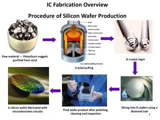
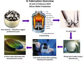
Processing line @ TMEC Furnace Cleaning Process Photolithography Down to 0.5μm Technology Implanter Metrology Plasma CVD Sputtering Dry Etching
Overview to Lithography process What is Lithography Process? The word come from the Greek “Lithos”and “Graphia” Lithos = Stones , Graphia = to write It means “ Writing on stones”. In Semiconductor, stones are Silicon wafersand our patterns are written with a light-sensitive polymer called “Photoresist”
Overview to Lithography process 9 Steps of Lithography process. 1. Wafer preparation 5. Post-Exposure Bake (PEB) 6. Development 2. Coat with Photoresist 7. Postbake, Hardbake 3. Prebake, Softbake 8. Etch or Implant 4. Align and Exposure 9. Photoresist strip
Photolithography Problem Without OPC With OPC Light Diffraction is occur during photolithography process. (a) (b) (c) (d) OPC patterns are used to reduce the error in photolithography process.
How to patterning circuit Processing - Film Deposition - Photolithography - Etching - Implantation Wafer Integrated Circuit (IC)
Processing line Silicon Wafer p-type wafer p-type
Processing line Film Deposition Initial oxidation: O2/H2 (Thickness: 420 nm) SiO2 p-type
Processing line Photolithography Coater Stepper Developer Photoresist (PR) p-type
Processing line Photoresist Characteristic PR is made up of a resin R, the photoactive compound M, the solvent S, and component appears during exposure which are exposure products P. The exposure products generated by the reaction of M with UV light.!! Applying Beer’s Law, the absorption coefficient is then, M0 = initial PAC concentration (non-exposed) A = bleachable absorption coefficients of Dill parameters B = Non-bleachable absorption coefficients of Dill parameters Other non-bleachable components of the PR such as dye are added to B
Processing line Dill Paramaters of Photoresist Where several assumptions are made in solving this differential equation and I x t is the optical dose. If D is the resist thickness, the Dill parameters can be measured by: T(∞) is transmittance at the air-resist interface T(0) T(0) is the transmittance of the unexposed resist, and T(∞) is the transmittance of the completely exposed resist is the initial slope of the transmittance vs dose curve Two transmittance curves for Kodak 820 resist 365 nm. The curves are for a convection oven post-apply bake of 30 minutes at the temperatures shown
Simulation of Plasma Etching Processing line Etching Photoresist (PR) Dry etch oxide p-type
Processing line Etching Directionality of Etcing Process Isotropic Etch Directional Etch Vertical Etch
Processing line Etching Two Kinds of Etching Method • by Wet chemical solution • Isotropic etching • by Plasma • Anisotropic etching Vertical E/R ~ Horizontal E/R Pure Chemical Reaction High Selectivity CD Loss or Gain Vertical E/R >> Horizontal E/R Ion assisted Relatively low Selectivity No CD bias
Processing line Implantation n-well implantation : Phosphorus Photoresist (PR) p-type
Processing line Chemical Mechanical Planarization (CMP) CMP removes material from uneven topography on a wafer surface until a flat (planarized)surface is created. CMP combines the chemical removal effect of an acidic or basic fluid solution with the "mechanical" effect provided by polishing with an abrasive material.
Processing line How to patterning a CMOS !!!