Download
1 / 21
210 likes | 374 Vues
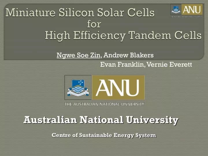
Miniature Silicon Solar Cells. for. High Efficiency Tandem Cells. Evan Franklin, Vernie Everett. Ngwe Soe Zin , Andrew Blakers. Australian National University. Centre of Sustainable Energy System. Outline. Purpose of the work Background of the Project

E N D
Miniature Silicon Solar Cells for High Efficiency Tandem Cells Evan Franklin, Vernie Everett NgweSoeZin, Andrew Blakers Australian National University Centre of Sustainable Energy System
Outline • Purpose of the work • Background of the Project • Silicon Solar Cells for VHESC program • Cell Design • Design Considerations • Target Efficiency • Modelling and Characterisation • Metal Plating • IV Test Data • Characterisation of Recombination • Conclusion
Purpose of the work • Ultra-High efficiency solar cell devices are a major step forward in the development of low-cost PV technology • Commercial applications, energy security, green house gas reductions, industry development • Military applications, pollution reduction • Potential trigger to revolutionise global electricity generation
Background • Single junction: 25% eff. in Si or GaAs (85% of practical efficiency) • Tandem: 38% for 3-stack under concentration (70% of practical efficiency) • Solar cell efficiencies are approaching their practical efficiency limits
Background • Very High Efficiency Solar Cell (VHESC) program works towards six-junction tandem solar cell stack approach • VHESC integrates optics, interconnects, and cell designs • Benefits: • Increased “design space” • Increased theoretical efficiency • Introduces options for new architectures • Greater device design flexibility • Reduced spectral mismatch losses • Increased materials choices • VHESC cells will be used in the mobile battery charging application
Background (6-junction Tandem Stack) 6-junction Solar Cell at 100 X 20 X 6J Solar Cell Band Gap Thermodynamic Efficiency Practical Efficiency Limit Practical Efficiency Limit High Eg 2.40 eV 14.9% 13.8% 13.8% GaInP 1.80 eV 16.6% 14.3% 14.3% GaAs 1.43 eV 13.9% 11.7% 12.0% Derating of thermodynamic efficiency IEEE Barnett et al 2006 Si 1.12 eV 9.7% 7.8% 8.5% 0.95 eV 5.0% 3.8% 4.0% 0.70 eV 4.1% 2.9% 3.0% Total η = 64.2% Total η = 54.3% Total η = 55.6%
Cell Design 0.15 mm 5.5 mm 0.3 mm 0.5 mm 2.5 mm 1.9 mm 0.3 mm 0.75 mm 0.75 mm 6.5 mm Emitter Region (n+) Base Region (p) • Bifacial Cell • N Contact at the Front • P Contact at the Back Metal Contact
Cell Design Considerations • Illumination • Light of energy <1.42eV to Silicon • Light of energy <1.1eV to underlying cells • BSR not an option • Cell thickness should be 0.5-2mm for reasonable conversion efficiency for 875-1100nm • IQE • Diffusion length >> Cell thickness for more than 90% IQE • Resistive Losses • 500µm thick cell will absorb 87% of the light (875-1100nm) in the top half of the cell • Current sharing in bifacial cell will minimise resistive losses partially • Electron current at the rear of diffused emitter will be small • Recombination • Thermal oxidation for Surface Recombination • Cutting cells individually from the host wafer for Edge Recombination • Contact is <1% of total surface area for Contact Recombination • Lateral Diffusive Losses • Electron resistive loss is more concerned than that of hole since Rs of 500µm 1Ωcm << Rs of Emitter Diffusion • For estimated resistive loss of <5%, n++ contacts will be at both edges and ends of the cell (similar configuration for p++ contacts) • Anti-Reflection • Optimisation of oxide and nitride thickness to reduce reflection loss of • 1% in air • 3% under encapsulation
Input Power Before High Band-Gap Materials = Input Power Before Silicon Material (875-1100nm) = = Target Efficiency 5.2% = 5.2% = Isc x Voc x FF Output Power of Cell = 6mA x 630mV x 78% Cell Efficiency High Eg Cell GaInP/GaAs 1.9 mm 1.9mm Silicon - +
Modelling • Main Parameters Used for Modelling • Active Area for 15mm • Illumination at 1 sun intensity • Bifacial Emitter as Active Region • Heavy Phosphorous and Boron Diffusions
Characterisation • Carrier lifetime after all high temperature step was maintained at around 560µs (~ implied-Voc of 640mV) • Surface recombination was also remained low at around 25 fA/sq cm QSSPC technique was used to characterise effective carrier lifetime and emitter saturation current.
Metallisation • metallisation of small contact with dimension of 200µm x 5.5mm • evaporated metal contacting method needs • Fabrication of selective mask with opening only to contacts can tedious • Alignment of mask to contact can be error-prone • Misalignment can cause shading loss and shunting
Metallisation • Light-induced plating for n++ contacts • Electrolyte plating for p+ contacts • Both plating performed concurrently
Metallisation AFM Rate of Plating p+ Contact n++ Contact Assuming the conditions: • Current generated by light enters in the emitter equally • Current enters the metal bus bar from one end and extracted from the other end Power Loss (%) Optical Microscope Measurement
Cells Making LPCVD Silicon Etch TMAH Etch RCA Clean Si Laser Scribe Diffusion Oxidation & LPCVD Etch for n++ Etch for n+ Strip SiN SiN n+ n+ n+ n+ Si n+ n+ n+ n+ Diffusion Oxidation Diffusion Etch for p+ Oxide Removal n+ n+ n+ n+ n+ n+ n+ n+ n+ n+ Metallisation n+ n+ Dicing
I-V Testing Tested by flash-tester under 1 sun illumination Demonstrates the absence of shunt and good fill-factor Low Voc and Isc could be due to recombination at the emitter and cell edge (cells diced out of host wafer) Recombination due to cell edge unlikely since active region is at least 1mm away from cell edge
Characterisation Recombination at the emitter region is suspected Experiment on dielectric using as etch mask and diffusion barrier
Characterisation Experiment on dry etching (RIE) if it has impact on lifetime Results were compared against the earlier results
Characterisation Samples deposited with nitride as etch mask or diffusion mask results in low lifetime compared to oxide Implied Voc was also observed lower for Sample using nitride as a etch mask Using nitride directly on top of silicon as etch mask or diffusion barrier may induce stress and thermal mismatch Samples etched by RIE to form emitter region has suffered drastic lifetime loss among all samples Ion damage caused by RIE on the silicon causes lifetime loss significantly
Conclusion Cells fabricated present the absence of shunting and good fill-factor Low Voc and Isc for cells Possible factors causing low Voc and Isc were identified Subsequent batch of cell fabrication could increase the cell efficiency sharply
Questions & Answers