Download
1 / 54
540 likes | 826 Vues
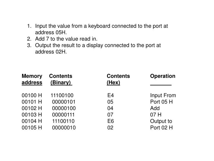
Input the value from a keyboard connected to the port at address 05H. Add 7 to the value read in. Output the result to a display connected to the port at address 02H. Memory Contents Contents Operation address (Binary) (Hex) 00100 H 11100100 E4 Input From

E N D
Input the value from a keyboard connected to the port at address 05H. • Add 7 to the value read in. • Output the result to a display connected to the port at address 02H. Memory Contents Contents Operation address(Binary) (Hex) 00100 H 11100100 E4 Input From 00101 H 00000101 05 Port 05 H 00102 H 00000100 04 Add 00103 H 00000111 07 07 H 00104 H 11100110 E6 Output to 00105 H 00000010 02 Port 02 H
SEQUENCE f. CPU sends out address of first instruction to memory g. CPU sends out memory ‘Read’ control signal to enable memory n. Instruction byte sent from memory to CPU on data bus (goes into instruction register IR of CPU) e. Address next memory location to get rest of the instruction h. Send memory ‘Read’ control signal to enable memory o. Port address byte sent from memory to CPU on data bus u. CPU sends out port address on address bus v. CPU sends out Input ‘Read’ control signal to enable port x. Data from port sent to CPU on data bus d. CPU sends address of next instruction to memory j. CPU sends memory ‘Read’ control signal to enable memory p. Instruction byte from memory sent to CPU on Data bus
c. CPU sends next address to memory to get rest of instruction k. CPU sends memory ‘Read’ control signal to enable memory q. Number 07 H sent from memory to CPU on data bus b. CPU sends address of next instruction to memory l. CPU sends memory ‘Read’ control signal to enable memory r. Instruction byte from memory sent to CPU on data bus a. CPU sends out next address to get rest of instruction m. CPU sends out memory ‘Read’ control signal to enable memory s. Port address byte sent from memory to CPU on data bus t. CPU sends out port address on address bus y. CPU sends out data to port on data bus w. CPU sends out Output ‘Write’ signal to enable port
Memory a b c d e f g h j k l m n o p q r s Control bus CPU Data bus Address bus Control bus t u x y v w I/O P O R T 0 5 P O R T 0 2 0 1 2 3 4 5 6 7 Display 8 9 + - Keyboard
Table. 1 Basic symbols for register-transfer logic Symbols Description Examples Capital letters and numerals Denotes a register A, MBR, R1 Subscript Denotes a bit of a register A2, Bi, B6 Parentheses ( ) Denotes a portion of a register PC(H) Arrow Denotes transfer of information A B Colon : Denotes termination of control function P : , x’T0 : Comma , Seperates two microoperations A B, B A Square brackets [ ] Specifies an address for memory transfer MBR M[MAR]
Select . x y 0 1 2 3 An A1 4x1 Mux No.1 4x1 Mux No.1 Load Register A . Bn B1 . . . . . . . . Register B . . Cn C1 Register C . . 0 1 2 3 4x1 Mux No.n Dn D1 Register D . Line No. n . n bus lines Line No.1 z 0 1 2 3 Select w Destination decoder Bus System for four registers E Enable
Output Control Bidirectional Bus Input Control Bus Si Control So Bus disabled (high impedance) Bi-directional bus buffer
Bus line for bit 0 A0 B0 C0 D0 S1 0 S0 1 2 E 2 x 4 3 Decoder Select Enable Bus line with three-state-buffers
Inputs A0 Read Memory unit A1 Address bus MUX A2 Data bus Write Outputs A3 Select B0 MUX Destination decoder B1 Select Select B2 B3 Memory that communicates with multiple registers
Arithmetic microoperations Symbolic Designation Description F A + B Contents of A plus B tranfered to F F A – B Contents of A minus B tranfered to F B B’ Compliment register B ( 1’s compliment ) B B’ + 1 Form the 2’s compliment of the contents of register B F A + B’ + 1 A plus the 2’s compliment of B transferred to F A A + 1 Increment the contents of A by 1 ( count up ) A A - 1 Decrement the contents of A by 1 ( count down )
Logic Microoperations Boolean funtions Microoperations Name F = 0 F 0 Clear F1 = xy F A . B AND F2 = xy’ F A . B’ F3 = x F A Transfer A F4 = x’y F A’ . B F5 = y F B Transfer B F6 = x(+) y F A (+) B Exclusive-OR F7 =x + y F A + B OR F8 = ( x + y )’ F ( A + B )’ NOR F9 = ( x (+) y )’ F ( A (+) B )’ Exclusive-NOR F10 = y’ F B’ Compliment B F11 = x + y’ F A + B’ F12 = x’ F A’ Compliment A F13 = x’ + y F A’ + B F14 = ( xy )’ F ( A + B )’ NAND F15 = 1 F All 1’s Set to all 1’s
Shift Microoperations Symbolic Description designation shl A Shift – left register A, contents of rigt-most flip flop becomes 0 Shr A Shift – right register A, contents of leftt-most flip flop becomes 0 Cil A Circulate left contents of register A Cir A Circulate right contents of register A ashl A Arithmetic shift- left contents of register A ashr A Arithmetic shift left contents of register A
A B A1 A2 A3 A4 B1 B2 B3 B4 S2 Mode select S1 Function select Cout S0 Output carry Cin Input Carry F4 F3 F2 F1 F Block diagram of a 4-bit ALU
Cin S1 Ci S0 A1 X1 B1 . (FA) F1 Y1 C2 A2 X2 B2 (FA) F2 Y2 C3 A3 X3 B3 (FA) F3 Y3 C4 A4 X4 B4 (FA) F4 Y4 Cout C5
Function X Y Output Functions Select Equals Equals Equals S2 S1 S0 Cin 0 0 0 0 A 0 F = A Transfer A 0 0 0 1 A 0 F = A+1 Increment A 0 0 1 0 A B F = A+B Add B to A 0 0 1 1 A B F = A+B+1 Add B to A plus 1 0 1 0 0 A B’ F = A+B’ Add 1’s compliment of B to A 0 1 0 1 A B’ F = A+B’+1 Add 2’s compliment of B to A 0 1 1 0 A All 1’s F = A-1 Decrement A 0 1 1 1 A All 1’s F = A Transfer A
Function Table Ai 4X1 MUX • S2 S1 S0 Output Operation • 0 0 Fi = Ai + Bi OR • 1 0 1 Fi = Ai (+) Bi XOR • 1 1 0 Fi = Ai . Bi And • 1 1 1 Fi = Ai NOT 0 Bi 1 Fi 2 3 S1 S0 Logic Diagram
Ci Ci+1 Ai One stage of arithmetic circuit Bi S1 2 X 1 MUX S0 0 S2 Fi 1 One stage of logic circuit S2
S2 S1 S0 Xi Yi Ci Fi = Xi (+) Yi Operation Req Function • 0 0 Ai 0 0 Fi = Ai Trasfer A OR • 0 1 Ai Bi 0 Fi = Ai (+) Bi XOR XOR • 1 0 Ai Bi’ 0 Fi = Ai (.) Bi Equivalence AND • 1 1 1 Ai 1 0 Fi = Ai’ NOT NOT
Cin S2 S1 S2’ C1 S0 S2S1S0’ S2S1’S0’ Z1 B1 X1 Full adder A1 F1 B1 B1 S0 Y1 B1’ S1 C2 S2’ Logic Diagram of ALU Z2
Function Output Functions Select S2 S1 S0 Cin 0 0 0 0 F = A Transfer A 0 0 0 1 F = A+1 Increment A 0 0 1 0 F = A+B Addition 0 0 1 1 F = A+B+1 Add with carry 0 1 0 0 F = A-B-1 Subtract with borrow 0 1 0 1 F = A-B Subtraction 0 1 1 0 F = A-1 Decrement A 0 1 1 1 F = A Transfer A 1 0 0 x F = A+B OR 1 0 1 x F = A(+)B XOR 1 1 0 x F = A.B And 1 1 1 x F = A’ Compliment A
Data bus CPU Power supply Clock output Interrupt Acknowledge Clock input Bus Granted Reset Read Interrupt request Write Bus Request Address bus Fig. Control signals in a microprocessor
Bidirectional data bus (DBUS) 8 1 Data buffers 8 bit internal bus Multiplexer Temporary register (T) Status register B C Instruction register (IR) D E F G Register select Program counter (PC) Stack pointer ALU Instruction decoder Address register (AR) H L Accumulator register (A) 16 9 8 1 Timing and control Address buffers Address bus (ABUS) RD (read) Other controls WR (Write) Fig. Block diagram of microprocessor
Memory 4096 x 16 15 12 11 0 Op code Address Instruction (program) Instruction format Operand (data) 15 0 Binary operand Processor register (Accumulator) Fig. Stored program organization
15 14 12 11 0 I Op code Address (a). Instruction format 22 457 1 ADD 457 35 300 1350 0 ADD 300 1350 Operand Operand AC AC (c). Indirect address (b). Direct address
Table. Partial list of instructions for mocroprocessor • Heaxa • decimal Instruction • code symbol Description Function • 78 MOV A,B Move B to A A B • 3E MVI Move immediate operand to A A D8 • 7E MOV A,FG Move to A with register indirect A M[FG] • 77 MOV FG,A Move A with register indirect M[FG] A • 3A LDA AD16 Load A direct A M[AD16] • 80 Add B ADD B to A A A + B • 86 SUB B Subtract B from A A A – B • A0 ANA B AND B to A A A.B • 04 INR B Increment B B B + 1 • 2F CMA Compliment A A A’ • 37 STC Set carry bit to 1 C 1 • C3 JMP AD16 Jump unconditionally PC AD16 • DA JC AD16 Jump on carry If (C=1) then • (PC AD16)
Fig. Numerical example for the call-subroutine and return-from-subroutine instructions. Stack Main program Subroutine 7800 PC 3500 CALL Op-code First op-code 2673 26 3501 Subroutine 73 3502 SP 46 7803 Return op-code 2686 Next op-code 3503 (a). Initial values PC First op-code 2673 CALL Op-code 3500 7800 Subroutine 26 3501 03 7801 SP 73 3502 35 7802 Return op-code 2686 Next op-code 3503 46 7803 (b). After execution of the CALL instruction First op-code CALL Op-code Subroutine 03 26 35 73 SP Return op-code 46 7803 PC Next op-code 3503 (c). After execution of RETURN instruction
Fig. Vectored Interrupt Configuration Interrupt source End of instruction execution 1 2 Interrupt request Interrupt acknowledge (INTACK) 3 4 IEN (DBUS) Interrupt vector Interrupt enable
Input Outputs • (Interrupt source) • ( Partial Address ) ( Interrupt request ) • I0 I1 I2 I3 x y R • x x x 0 0 1 • 0 1 x x 0 1 1 • 0 0 1 x 1 0 1 • 0 0 0 1 1 1 1 Fig. Priority encoder truth table
Chip select 1 Chip select 2 CS1 CS2’ 128x8 RAM Fig. Block diagram of a RAM chip Read Write 7-bit address RD WR AD7 8-bit data bus Fig. Function table of RAM chip CS1 CS2’ RD WR Memory function State of data bus 0 0 x x Inhibit High impedance 0 1 x x Inhibit High impedance 1 0 0 0 Inhibit High impedance 1 0 0 1 Write Input data to RAM 1 0 1 x Read Output data from RAM 1 1 x x Inhibit High impedance CS1 512x8 ROM CS2’ AD9 Chip select 1 Chip select 2 8-bit Data bus 9-bit address Fig. Block diagram
Table. Memory address map for microcomputer Address bus Hexadecimal address Component 10 9 8 7 6 5 4 3 2 1 RAM 1 0000-007F 0 0 0 x x x x x x x RAM 2 0080-00FF 0 0 1 x x x x x x x RAM 3 0100-017F 0 1 0 x x x x x x x RAM 4 0180-01FF 0 1 1 x x x x x x x ROM 0200-03FF 1 x x x x x x x x x
Microprocessor Address bus 16-11 10 9 8 7-1 RD WR Data bus Decoder 3 2 1 0 CS1 128x8 CS2’ RAM1 RD WR Data AD7 CS1 128x8 CS2’ RAM2 RD WR Data AD7 CS1 128x8 CS2’ RAM3 RD WR Data AD7 CS1 128x8 CS2’ RAM4 RD WR Data AD7 CS1 512x8 CS2’ ROM Data AD9 1-7 8 9 Fig. Memory connection to the microprocessor
CPU address ( 15 bits) Argument register Address Data 0 1 0 0 0 3 4 5 0 0 2 7 7 7 6 7 1 0 2 2 3 4 5 1 2 3 4 Fig. The Associative Mapping cache
6-bits 9-bits Tag Index 0 0 0 0 0 0 0 0 32K x 12 Main memory Address = 15 bits Data = 12 bits 512 x 12 Cache memory Address = 9 bits Data = 12 bits Octal address Octal address 7 7 7 7 7 7 7 7 Fig. Addressing relationships between main and cache memories
Memory address Index address Memory data Tag Data 1 2 2 0 2 3 4 0 3 4 5 0 4 5 6 0 5 6 7 0 6 7 1 0 0 0 0 0 0 1 2 2 0 0 2 6 7 1 0 0 0 0 0 0 0 0 7 7 7 0 1 0 0 0 7 7 7 0 1 7 7 7 (b). Cache memory 0 2 0 0 0 0 2 7 7 7 (a). Main memory Fig. Direct Mapping cache organization
Index Tag Data Tag Data 0 0 0 0 1 3 4 5 0 0 2 5 6 7 0 7 7 7 0 2 6 7 1 0 0 0 2 3 4 0 Fig. Set-associative mapping cache with set size of two.
Auxiliary memory Program 1 Data 1, 1 Data 1, 2 Program 2 Data 2, 1 Program 1 Data 1, 1 Memory space M = 32 K = 2¹ˢ Address space N = 1024 K = 2²º Fig. Relationship between address and memory space in a virtual memory system.
Page 0 Page 1 Page 2 Page 3 Page 4 Block 0 Page 5 Block 1 Page 6 Block 2 Page 7 Block 3 Address space N = 8 k = 2¹³ Memory space M = 4 K = 2¹² Fig. Address space and memory spsce split into groups of 1 k words.
Page No. Line number Virtual address 1 0 1 0 1 0 1 0 1 0 0 1 1 Presence bit Table address 0 0 0 0 1 1 1 0 0 1 Main memory 0 0 1 0 1 0 Block 0 0 0 1 1 Block 1 0 1 0 1 0 1 0 1 0 0 1 1 0 1 0 0 Block 2 0 1 1 1 0 1 Main memory address register Block 3 1 0 1 1 1 0 0 1 1 1 MBR 0 1 1 Memory page table buffer register Fig. Memory table in a paged system.
Instruction register (IR) 11 - 0 Other inputs 15 14 13 12 Control logic gates 3 X 8 decoder . . . D0 I Control outputs 7 6 5 4 3 2 1 0 D7 . . . T15 T0 15 14 2 1 0 4 X 16 decoder Control Unit of basic computer Increment (INR) 4- bit Sequence counter (SC) Clear (CLR) Clock
Control word Next address generator (Sequencer) Control address register Control memory (ROM) Control data register External input Next address information Fig. Microprogrammed control organization
Instruction code Mapping logic Subroutine Register (SBR) Branch logic MUX select Multiplexers Status bits Control address register (CAR) Clock Incrementer Control Memory Select a status bit Micro operations Branch address Fig. Selection of address for control memory
Data bus Bus buffers I/O bus Port A data register CS RS1 RS2 RD WR Interrupt Reset Chip select and read/write control Port A control register Handshake lines Internal bus I/O bus Port B data register Port B control register Handshake lines CS RS1 RS2 Register select 0 x x None – data bus in high impedance 1 0 0 Port A data register 1 0 1 Port A control register 1 1 0 Port B data register 1 1 1 Port B control register Fig. Block diagram of parallel peripheral interface.
Data Bus Bus buffers Transmit Shift register Transmitter Register CS RS RD WR Chip select and read/write control data Transmitter Control register Transmitter control and clock clock Internal bus Status register Receiver control and clock Receiver clock Shift register Receiver register Receive data Reset CS RS Operation Register selected 0 x x None 1 0 WR Transmitter register 1 1 WR Control register 1 0 RD Receiver register 1 1 RD Status register Fig. Block diagram of a typical serial communication interface.
Data Bus Data bus buffers Address bus Address bus buffers CS RS1 RS2 WR RD Chip select and read/write control Address register Internal bus Byte count register BR BG Control register DMA request DMA Acknowledge Reset Read / write Interrupt Fig. Block diagram of DMA controller
Bi Ci Ai R1 R2 Multiplier R3 R4 Adder Fig. Example of parallel processing R5
Data Bus Bus buffers Transmit Shift register Transmitter Register CS RS RD WR Chip select and read/write control data Transmitter Control register Transmitter control and clock clock Internal bus Status register Receiver control and clock Receiver clock Shift register Receiver register Receive data Reset CS RS Operation Register selected 0 x x None 1 0 WR Transmitter register 1 1 WR Control register 1 0 RD Receiver register 1 1 RD Status register Fig. Block diagram of a typical serial communication interface.
Table: Content of registers in pipeline example • Clock Segment1 Segment2 Segment3 • pulse • number R1 R2 R3 R4 R5 • A1 B1 • A2 B2 A1 * B1 C1 • 3 A3 B3 A2 * B2 C2 A1 * B1 + C1 • A4 B4 A3 * B3 C3 A2 * B2 + C2 • 5 A5 B5 A4 * B4 C4 A3 * B3 + C3 • 6 A6 B6 A5 * B5 C5 A4 * B4 + C4 • 7 A7 B7 A6 * B6 C6 A5 * B5 + C5 • 8 A7 * B7 C7 A6 * B6 + C6 • 9 A7 * B7 + C7
Fig. Pipeline for floating-point addition and subtraction Exponents a b Mantissas A B R R Compare exponents by subtraction Difference Segment 1: R Align mantissas Segment 2: Choose exponent R Add or subtract mantissas Segment 3: R R Normalize result Adjust exponent Segment 4: R R
Bs multiplicand B register Sequence counter (SC) Complementer and parallel adder (rightmost bit ) Qn As Qs 0 E A register Q register multiplier Fig. Hardware for multiply operation
Multiplcand in B Multiplier in Q Fig. Flow chart for multiply algorithm As Qs (+) Bs Qs Qs (+) Bs A 0, E 0 SC n-1 = 0 = 1 Qn EA A + B Shr EAQ SC SC-1 = 0 Not equal to zero SC END (product in reg A & Q)