Download
1 / 43
490 likes | 686 Vues
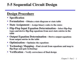
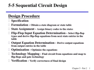
Sequential Circuit Design. Design Procedure. Specification Formulation Obtain a state diagram or state table State Assignment Assign binary codes to the states Flip-Flop Input Equation Determination Select flip-flop types Derive flip-flop equations from next state entries in the table

E N D
Design Procedure • Specification • Formulation • Obtain a state diagram or state table • State Assignment • Assign binary codes to the states • Flip-Flop Input Equation Determination • Select flip-flop types • Derive flip-flop equations from next state entries in the table • Output Equation Determination • Derive output equations from output entries in the table • Optimization • Optimize the equations • Technology Mapping • Find circuit from equations and map to flip-flops and gate technology • Verification • Verify correctness of final design
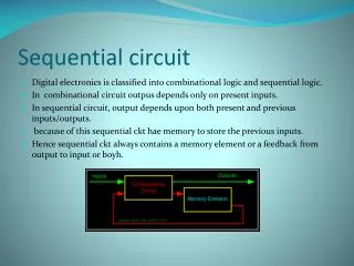
Typical Sequential Circuit Mealy Machine C1 C2 s(t+1) State Register next state s(t) z(t) present state x(t) present inputs clock
x A Q D A’ Q C Next State B Q D CP Q' C y Output Typical Sequential Circuit Example
Sequence Detector • 101 sequence Detector
1/0 Design of 101 Sequence Detector • State Diagram:
Design of 101 Sequence Detector • State Diagram (final):
Design of 101 Sequence Detector • State Table: • State Table with State Assignment: DA DB
A A A A A B B B 00 01 11 10 00 01 11 10 X X 0 0 1 X 0 0 0 0 X 0 1 0 0 X 0 1 1 1 X 1 B B DA = X’.B DB = X A 00 01 11 10 0 0 0 X 0 0 1 0 X 1 Z = X.A B Design of Sequence Detector • Derive Boolean Equations:
C1 C2 State Register s(t+1) next state s(t) present state x(t) z(t) present inputs clock Design of Sequence Detector Compare with Typical Mealy Machine
Design of Sequence Detector • A Moore Sequence Detector: C2 C1 z(t) s(t+1) State Register next state s(t) present state x(t) present inputs clock
Sequence Detector • 101 sequence Detector
Design of a Sequence Detector S0: start S1: got 1 S2: got 10 S3: got 101
Design of a Sequence Detector S0: start S1: got 1 S2: got 10 S3: got 101
Design of a Sequence Detector State Table Transition Table with State assignment DA DB
State Assignment • Each of the m states must be assigned a unique code. • Minimum number of bits required is n such thatn ≥ log2 mwhere x is the smallest integer ≥ x. • There are 2n - m unused states. • (There are useful state assignments that use more than the minimum number of bits).
Present Next State Output State x=0 x=1 x=0 x=1 A A B 0 0 B A C 0 0 C D C 0 0 D A B 0 1 State Assignment: Example 2 • How may assignments of codes with a minimum number of bits? • 4 3 2 1 = 24 • Does code assignment make a difference in cost?
State Assignment: Example 2 • Assignment 1: • A = 0 0, B = 0 1, C = 1 0, D = 1 1 • The resulting coded state table:
State Assignment: Example 2 • Assignment 2: • A = 0 0, B = 0 1, C = 1 1, D = 1 0 • The resulting coded state table:
A A B B A 00 01 11 10 X 0 0 0 0 1 1 0 1 0 1 B DA = A.B’ + X.A’.B Flip-Flop Input and Output Equations: Example 2 (version 1) • Assume D flip-flops • Interchange the bottom two rows of the state table, to obtain K-maps for DA, DB, and Z: A 00 01 11 10 X 0 0 0 0 1 1 1 0 1 0 B DB = X’.A.B’ + X.A’.B’+X.A.B
A B Flip-Flop Input and Output Equations: Example 2 (version 1) A 00 01 11 10 X 0 0 0 0 0 1 0 0 1 0 B Z = A.B.X Gate Input Cost = 22
A A B B Flip-Flop Input and Output Equations: Example 2 (version 2) • Assume D flip-flops • Interchange the bottom two rows of the state table, to obtain K-maps for DA, DB, and Z: A A 00 01 11 10 00 01 11 10 X X 0 0 0 1 0 0 0 0 0 0 1 0 1 1 0 1 1 1 1 1 B B DA = A.B + X.B DB = X
A B Flip-Flop Input and Output Equations: Example 2 (version 2) A 00 01 11 10 X 0 0 0 0 0 1 0 0 0 1 B Z = A.B’.X Gate Input Cost = 9 Select this state assignment
Y1 D C R Z Y2 D X Clock C R Reset Implementation • Initial Circuit: • Library: • D Flip-flopswith Reset(not inverted) • NAND gateswith up to 4inputs andinverters
Y1 D C R Z Y2 D X C Clock R Reset Technology Mapping
Example : Vending Machine • General Machine Concept: • Deliver package of gum after 15 cents deposited • Single coin slot for dimes (10¢) , nickels (5¢) • No change
5¢ Coin Vending Gum Open 10¢ Sensor Machine Release FSM Mechanism Reset Clk Example : Vending Machine • Step 1: Understand the problem: • Draw a picture
Reset S0 N D S1 S2 D N D N S4 S6 S3 S5 [open] [open] [open] N D S7 S8 [open] [open] Example : Vending Machine • Step 2: Draw state diagram: • All possible sequences • Inputs: N, D, reset • Output: open Dime: 10¢ Nickel: 5¢ • Notes: • If neither N nor D, goes to itself. • Both N and D is not possible.
Reset 0¢ D N 5¢ D N 10¢ N, D 15¢ [open] Example : Vending Machine • Step 3: State minimization: • reuse states whenever possible Dime: 10¢ Nickel: 5¢
Present Next Output State D N State Open 0¢ 0 0 0¢ 0 Reset 0 1 5¢ 0 0¢ 1 0 10¢ 0 1 1 X X D N 5¢ 0 0 5¢ 0 5¢ 0 1 10¢ 0 1 0 15¢ 0 1 1 X X D N 10¢ 0 0 10¢ 0 10¢ 0 1 15¢ 0 1 0 15¢ 0 N, D 1 1 X X 15¢ 15¢ X X 15¢ 1 [open] Example : Vending Machine • Step 4: Symbolic State table: Inputs From 15¢ state, you may want to go to reset state
Present State Next State Output Q Q D N D D Open 1 0 1 0 0 0 0 0 0 0 0 0 1 0 1 0 1 0 1 0 0 1 1 X X X 0 1 0 0 0 1 0 0 1 1 0 0 1 0 1 1 0 1 1 X X X 1 0 0 0 1 0 0 0 1 1 1 0 1 0 1 1 0 1 1 X X X 1 1 0 0 1 1 1 0 1 1 1 1 1 0 1 1 1 1 1 X X X Example : Vending Machine • Step 5: State encoding: Inputs
Q1 Q1 Q1 Q1 Q0 Q1 Q0 Q1 Q0 D N D N D N 0 1 1 0 0 0 1 1 0 0 1 0 1 0 1 1 0 0 1 0 0 1 1 1 N N N X X X X X X X X X X X X D D D 1 1 1 1 0 1 1 1 0 0 1 0 Q0 Q0 Q0 K-map for D1 K-map for D0 K-map for Open Q 1 D Q D D Q 1 1 CLK \ Q Q Q 1 R 0 N \reset N OPEN \ Q 0 Q 0 \ N D Q D Q 0 0 Q CLK \ Q 1 Q 0 N R \reset Q 1 D Example : Vending Machine • Step 6: Choose FF for implementation: • DFF easiest D1 = Q1 + D + Q0 N D0 = N Q0’ + Q0 N’ + Q1 N + Q1 D OPEN = Q1 Q0 8 Gates
Using Other FFs for Design • Characteristic Table: • defines the next state of the flip-flop in terms of flip-flop inputs and current state. • Used in Circuit Analysis • Excitation Table: • defines the flip-flop input variable values as function of the current state and next state. • Used in Circuit Design
SR FF Tables • Characteristic Table: S R Q(t + 1) Operation 0 0 Q(t) No change 0 1 0 Reset 1 0 1 Set 1 1 ? Undefined • Excitation Table: Q(t) Q(t+ 1) S R Operation 0 0 0 X No change / Reset 0 1 1 0 Set 1 0 0 1 Reset 1 1 X 0 No change / Set
D Q(t 1) Operation + 0 0 Reset 1 1 Set DFF Tables • Characteristic Table: • Excitation Table: Q(t) Q(t+ 1) D 0 0 0 0 1 1 1 0 0 1 1 1
JK FF Tables • Characteristic Table: J K Q(t+1) Operation 0 0 Q(t) No change 0 1 0 Reset 1 0 1 Set 1 1 Complement Q(t) • Excitation Table: Q(t) Q(t+1) J K Operation 0 0 0 X No change / Reset 0 1 1 X Set / Toggle 1 0 X 1 Reset / Toggle 1 1 X 0 No Change / Set
T FF Tables • Characteristic Table: T Q(t+1) Operation 0 Q(t) No change 1 Q(t) Complement • Excitation Table: Q(t) Q(t+1) T Operation 0 0 0 No change 0 1 1 Toggle 1 0 1 Toggle 1 1 0 No Change
Example • Design by DFF
Example A(t + 1) = DA(A,B,X) = m(2,4,5,6) B(t + 1) = DB(A,B,X) = m(1,3,5,6) Y(A,B,X) = m(1,5) BX BX A A DA = AB + BX DB = AX + BX + ABX BX A Y = BX
Example • Logic Diagram for Circuit with D Flip-Flops
Q(t) Q(t+1) J K Operation 0 0 0 X No change/reset 0 1 1 X Set/Toggle 1 0 X 1 Reset/Toggle 1 1 X 0 No Change/set Example • Design by JK FF • Don’t cares • lead to simpler combinational circuit
Example: Boolean Equations JA = BX JB = X KA = BX KB = AX + AX