Download
1 / 39
390 likes | 518 Vues
RISC Pipeline. Han Wang CS3410, Spring 2010 Computer Science Cornell University. See: P&H Chapter 4.6. Homework 2. 0 1 2 3 4 5 6 7 8 9. Announcements Homework 2 due tomorrow midnight Programming Assignment 1 release tomorrow Pipelined MIPS processor (topic of today)

E N D
RISC Pipeline Han Wang CS3410, Spring 2010 Computer Science Cornell University See: P&H Chapter 4.6
Homework 2 0 1 2 3 4 5 6 7 8 9
Announcements • Homework 2 due tomorrow midnight • Programming Assignment 1 release tomorrow • Pipelined MIPS processor (topic of today) • Subset of MIPS ISA • Feedback • We want to hear from you! • Content?
Absolute Jump Prog. Mem Reg.File inst ALU addr 5 5 5 =? PC Data Mem control cmp + +4 +4 offset imm ext tgt Could have used ALU for link add ||
A Processor Review: Single cycle processor memory registerfile inst alu +4 +4 addr =? PC din dout control cmp offset memory new pc target imm extend
Single Cycle Processor • Advantages • Single Cycle per instruction make logic and clock simple • Disadvantages • Since instructions take different time to finish, memory and functional unit are not efficiently utilized. • Cycle time is the longest delay. • Load instruction • Best possible CPI is 1
Pipeline Hazards 0h 1h 2h 3h…
A Processor memory registerfile inst alu +4 addr PC din dout control memory new pc computejump/branchtargets imm extend Write-Back InstructionDecode InstructionFetch Memory Execute
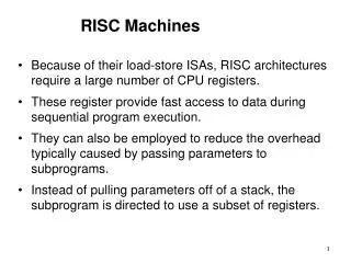
Basic Pipeline Five stage “RISC” load-store architecture • Instruction fetch (IF) • get instruction from memory, increment PC • Instruction Decode (ID) • translate opcode into control signals and read registers • Execute (EX) • perform ALU operation, compute jump/branch targets • Memory (MEM) • access memory if needed • Writeback (WB) • update register file Slides thanks to Sally McKee & Kavita Bala
Pipelined Implementation • Break instructions across multiple clock cycles (five, in this case) • Design a separate stage for the execution performed during each clock cycle • Add pipeline registers to isolate signals between different stages
Pipelined Processor memory registerfile A alu D D B +4 addr PC din dout B M inst control memory computejump/branchtargets newpc extend imm Write-Back InstructionDecode InstructionFetch ctrl ctrl ctrl Memory Execute IF/ID ID/EX EX/MEM MEM/WB
IF • Stage 1: Instruction Fetch • Fetch a new instruction every cycle • Current PC is index to instruction memory • Increment the PC at end of cycle (assume no branches for now) • Write values of interest to pipeline register (IF/ID) • Instruction bits (for later decoding) • PC+4 (for later computing branch targets) • Anything needed by later pipeline stages • Next stage will read this pipeline register
IF instructionmemory 1 WE addr mc inst 00 = read word +4 Rest of pipeline PC+4 1 PC pcreg newpc pcrel pcabs pcsel IF/ID
ID • Stage 2: Instruction Decode • On every cycle: • Read IF/ID pipeline register to get instruction bits • Decode instruction, generate control signals • Read from register file • Write values of interest to pipeline register (ID/EX) • Control information, Rd index, immediates, offsets, … • Contents of Ra, Rb • PC+4 (for computing branch targets later)
result ID dest registerfile WE A A Rd D B B Rb Ra decode inst Stage 1: Instruction Fetch Rest of pipeline imm extend PC+4 PC+4 ctrl IF/ID ID/EX
EX • Stage 3: Execute • On every cycle: • Read ID/EX pipeline register to get values and control bits • Perform ALU operation • Compute targets (PC+4+offset, etc.) in case this is a branch • Decide if jump/branch should be taken • Write values of interest to pipeline register (EX/MEM) • Control information, Rd index, … • Result of ALU operation • Value in case this is a memory store instruction
pcsel EX branch? pcreg A D alu B imm B Stage 2: Instruction Decode Rest of pipeline + pcrel PC+4 || pcabs ctrl ctrl ID/EX EX/MEM
MEM • Stage 4: Memory • On every cycle: • Read EX/MEM pipeline register to get values and control bits • Perform memory load/store if needed • address is ALU result • Write values of interest to pipeline register (MEM/WB) • Control information, Rd index, … • Result of memory operation • Pass result of ALU operation
MEM D D addr B M din dout Stage 3: Execute Rest of pipeline memory mc ctrl ctrl EX/MEM MEM/WB
WB • Stage 5: Write-back • On every cycle: • Read MEM/WB pipeline register to get values and control bits • Select value and write to register file
WB result D M Stage 4: Memory dest ctrl MEM/WB
instmem A A Rd D D D B B inst addr Rb Ra B M dout din imm +4 mem PC+4 PC+4 PC Rd Rd Rd OP OP OP ID/EX EX/MEM MEM/WB IF/ID
add r3, r1, r2; nand r6, r4, r5; lw r4, 20(r2); add r5, r2, r5; sw r7, 12(r3);
sw r7, 12(r3) sw r7, 12(r3) add r5, r2, r5 sw r7, 12(r3) add r5, r2, r5 lw r4, 20(r2) sw r7, 12(r3) add r5, r2, r5 lw r4, 20(r2) nand r6, r4, r5 sw r7, 12(r3) add r5, r2, r5 lw r4, 20(r2) nand r6, r4, r5 add r3, r1, r2 add r5, r2, r5 lw r4, 20(r2) nand r6, r4, r5 add r3, r1, r2 lw r4, 20(r2) nand r6, r4, r5 add r3, r1, r2 nand r6, r4, r5 add r3, r1, r2 add r3, r1, r2 instmem 0:add1:nand2:lw3:add4:sw A A Rd D D D B B inst addr Rb Ra 77 B M dout din imm +4 mem r0r1r2r3r4r5r6r7 0 36 9 12 18 7 41 22 PC+4 PC+4 PC Rd Rd Rd OP P OP ID/EX EX/MEM MEM/WB IF/ID
Time Graphs Clock cycle IF ID EX MEM WB IF ID EX MEM WB IF ID EX MEM WB IF ID EX MEM WB IF ID EX MEM WB Latency: Throughput: Concurrency: CPI =
Pipelining Recap • Powerful technique for masking latencies • Logically, instructions execute one at a time • Physically, instructions execute in parallel • Instruction level parallelism • Abstraction promotes decoupling • Interface (ISA) vs. implementation (Pipeline)
Sample Code (Simple) • Assume eight-register machine • Run the following code on a pipelined datapath add 3 1 2 ; reg3 = reg 1 + reg 2 nand6 4 5 ; reg6 = ~(reg 4 & reg 5) lw4 20 (2) ; reg4 = Mem[reg2+20] add 5 2 5 ; reg5 = reg 2 + reg 5 sw 7 12(3) ; Mem[reg3+12] = reg 7 Slides thanks to Sally McKee
+ A L U M U X 1 target PC+1 PC+1 0 R0 R1 regA ALU result R2 Register file regB valA M U X PC Inst mem Data mem instruction R3 ALU result mdata R4 valB R5 R6 M U X data R7 offset dest valB Bits 0-2 dest dest dest Bits 15-17 M U X Bits 21-23 op op op ID/EX EX/MEM MEM/WB IF/ID
+ A L U M U X 1 0 0 0 0 R0 0 36 R1 0 9 R2 Register file 0 M U X PC Inst mem Data mem nop 12 R3 0 0 18 R4 7 0 R5 41 R6 M U X data 22 R7 0 dest 0 Initial State Bits 0-2 0 0 0 Bits 15-17 M U X Bits 21-23 nop nop nop ID/EX EX/MEM MEM/WB IF/ID
+ A L U add 3 1 2 M U X 1 0 1 0 0 R0 0 36 R1 0 9 R2 Register file 0 M U X PC Inst mem Data mem add 3 1 2 12 R3 0 0 18 R4 7 0 R5 41 R6 M U X data 22 R7 0 dest 0 Fetch: add 3 1 2 Bits 0-2 0 0 0 Bits 15-17 M U X Bits 21-23 nop nop nop ID/EX EX/MEM MEM/WB IF/ID Time: 1
+ A L U nand 6 4 5 add 3 1 2 M U X 1 0 2 1 0 R0 0 36 R1 1 0 9 R2 Register file 2 36 M U X PC Inst mem Data mem nand 6 4 5 12 R3 0 0 18 R4 7 9 R5 41 R6 M U X data 22 R7 3 dest 0 Fetch: nand 6 4 5 Bits 0-2 3 0 0 Bits 15-17 M U X Bits 21-23 add nop nop ID/EX EX/MEM MEM/WB IF/ID Time: 2
+ A L U lw 4 20(2) nand 6 4 5 add 3 1 2 M U X 1 4 3 2 0 R0 0 36 R1 4 0 36 9 R2 Register file 5 18 M U X PC Inst mem Data mem lw 4 20(2) 12 R3 45 0 18 R4 9 7 7 R5 41 R6 M U X data 22 R7 6 dest 9 Fetch: lw 4 20(2) Bits 0-2 3 6 3 0 Bits 15-17 M U X Bits 21-23 nand add nop ID/EX EX/MEM MEM/WB IF/ID Time: 3
+ A L U add 5 2 5 lw 4 20(2) nand 6 4 5 add 3 1 2 M U X 1 8 4 3 0 R0 0 36 R1 2 45 18 9 R2 Register file 4 9 M U X PC Inst mem Data mem add 5 2 5 12 R3 -3 0 18 R4 45 7 7 18 R5 41 R6 M U X data 22 R7 20 dest 7 Fetch: add 5 2 5 Bits 0-2 3 6 4 6 3 Bits 15-17 M U X Bits 21-23 lw nand add ID/EX EX/MEM MEM/WB IF/ID Time: 4
+ A L U sw 7 12(3) add 5 2 5 lw 4 20 (2) nand 6 4 5 add 3 1 2 M U X 1 23 5 4 0 R0 0 45 36 R1 2 -3 9 9 R2 Register file 5 9 M U X PC Inst mem Data mem sw 7 12(3) 45 R3 29 0 18 R4 -3 7 7 R5 41 R6 M U X data 22 R7 20 5 dest 18 Fetch: sw 7 12(3) Bits 0-2 6 3 4 5 4 6 Bits 15-17 M U X Bits 21-23 add lw nand ID/EX EX/MEM MEM/WB IF/ID Time: 5
+ A L U sw7 12(3) add 5 2 5 lw 4 20(2) nand 6 4 5 M U X 1 9 5 0 R0 0 -3 36 R1 3 29 9 9 R2 Register file 7 45 M U X PC Inst mem Data mem 45 R3 16 99 18 R4 29 7 7 22 R5 -3 R6 M U X data 22 R7 12 dest 7 No more instructions Bits 0-2 4 6 5 7 5 4 Bits 15-17 M U X Bits 21-23 sw add lw ID/EX EX/MEM MEM/WB IF/ID Time: 6
+ A L U nopnopsw 7 12(3) add 5 2 5 lw 4 20(2) M U X 1 15 0 R0 0 36 R1 16 45 9 R2 Register file M U X PC Inst mem Data mem 45 R3 99 57 0 99 R4 16 7 R5 -3 R6 M U X data 22 R7 12 dest 22 No more instructions Bits 0-2 5 4 7 7 5 Bits 15-17 M U X Bits 21-23 sw add ID/EX EX/MEM MEM/WB IF/ID Time: 7
+ A L U nopnopnopsw7 12(3) add 5 2 5 M U X 1 0 R0 16 36 R1 57 9 R2 Register file M U X PC Inst mem Data mem 45 R3 0 99 22 R4 57 16 R5 -3 R6 M U X data 22 R7 dest 22 No more instructions Bits 0-2 5 7 Bits 15-17 M U X Bits 21-23 sw ID/EX EX/MEM MEM/WB IF/ID Time: 8 Slides thanks to Sally McKee
+ A L U nopnopnopnopsw 7 12(3) M U X 1 0 R0 36 R1 9 R2 Register file M U X PC Inst mem Data mem 45 R3 99 R4 16 R5 -3 R6 M U X data 22 R7 dest No more instructions Bits 0-2 Bits 15-17 M U X Bits 21-23 ID/EX EX/MEM MEM/WB IF/ID Time: 9