Download
1 / 21

E N D
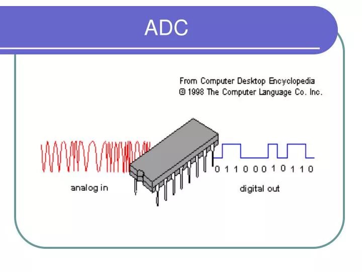
ADC • A/D converter (Analog/Digital converter) A device that converts continuously varying analog signals from instruments and sensors that monitor conditions, such as sound, movement and temperature into binary code for the computer. The A/D converter may be contained on a single chip or can be one circuit within a chip. See codec.
ADC • A/D Converters Are Everywhere Every digital desk phone and cellphone has an A/D converter that converts the pressure of sound waves into PCM code. Every digital camera, camcorder or scanner uses A/D converters to transform the variable charges in CCD and CMOS chips into the binary data that represent pixels
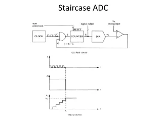
ADC • Analog-to-Digital or A/D conversion, the process of changing continuously varying data, such as voltage, current, or shaft rotation, into discrete digital quantities that represent the magnitude of the data compared to a standard or reference at the moment the conversion is made.
ADC • There are two types of converters: electromechanical—also called shaft- or position-to-digital—and electronic. The most common use is to change analog signals into a form that can be manipulated by a digital computer, as in data communications; a modem, or data set, is a device that converts the digital signals produced by computers and terminals into analog signals that telephone circuits are designed to carry and then back to digital signals at the other end of the communication link.
ADC • Similarly, in digital sound recording, audio signals are transformed into digital data, which are then recorded on a magnetic or optical disk or tape; the digitized data on the recording medium then must be changed back into the analog sound signals that can be used by a stereophonic sound system. See also digital-to-analog conversion.
ADC Flash ADC Also called the parallel A/D converter, this circuit is the simplest to understand. It is formed of a series of comparators, each one comparing the input signal to a unique reference voltage. The comparator outputs connect to the inputs of a priority encoder circuit, which then produces a binary output. The following illustration shows a 3-bit flash ADC circuit:
ADC • Vref is a stable reference voltage provided by a precision voltage regulator as part of the converter circuit, not shown in the schematic. As the analog input voltage exceeds the reference voltage at each comparator, the comparator outputs will sequentially saturate to a high state. The priority encoder generates a binary number based on the highest-order active input, ignoring all other active inputs.
Flash ADC When operated, the flash ADC produces an output that looks something like this:
Circuit ADC • For this particular application, a regular priority encoder with all its inherent complexity isn't necessary. Due to the nature of the sequential comparator output states (each comparator saturating "high" in sequence from lowest to highest), the same "highest-order-input selection" effect may be realized through a set of Exclusive-OR gates, allowing the use of a simpler, non-priority encoder:
DAC • This DAC circuit, otherwise known as the binary-weighted-input DAC, is a variation on the inverting summer op-amp circuit. If you recall, the classic inverting summer circuit is an operational amplifier using negative feedback for controlled gain, with several voltage inputs and one voltage output. The output voltage is the inverted (opposite polarity) sum of all input voltages:
DAC Circuit • Starting from V1 and going through V3, this would give each input voltage exactly half the effect on the output as the voltage before it. In other words, input voltage V1 has a 1:1 effect on the output voltage (gain of 1), while input voltage V2 has half that much effect on the output (a gain of 1/2), and V3 half of that (a gain of 1/4). These ratios are not arbitrarily chosen: they are the same ratios corresponding to place weights in the binary numeration system. If we drive the inputs of this circuit with digital gates so that each input is either 0 volts or full supply voltage, the output voltage will be an analog representation of the binary value of these three bits.
Binary Equivalent values • Binary | Output voltage | 000 0.00 V 001 -1.25 V 010 -2.50 V 011 -3.75 V 100 -5.00 V 101 -6.25 V 110 -7.50 V 111 -8.75 V